NJL7302L-F3/F5
advertisement
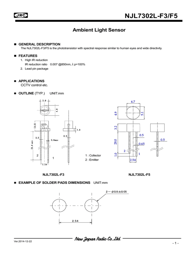
NJL7302L-F3/F5 Ambient Light Sensor GENERAL DESCRIPTION The NJL7302L-F3/F5 is the phototransistor with spectral response similar to human eyes and wide directivity. FEATURES 1. High IR reduction IR reduction ratio 0.007 @850nm,λp=100% 2. Lead pin package APPLICATIONS CCTV control etc. OUTLINE (TYP.) UNIT:mm 5.1 3.2 4.9 4.7 0.5 28.0 0.5 0.65 2 1 : Collector 2 : Emitter 1 1 1.0 2 2.54 NJL7302L-F3 NJL7302L-F5 EXAMPLE OF SOLDER PADS DIMENSIONS UNIT:mm 2-φ0. 8±0. 05 2. 54 Ver.2014-12-22 -1- NJL7302L-F3/F5 ABSOLUTE MAXIMUM RATINGS (Ta=25°C) PARAMETER Collector - Emitter Voltage Emitter - Collector Voltage Power Dissipation Operating Temperature Storage Temperature Soldering Temperature SYMBOL VCEO VECO PD Topr Tstg Tsol RATINGS 15 3 150 −30 to +70 −40 to +100 260 ELECTRO-OPTICAL CHARACTERISTICS UNIT V V mW °C °C °C SYMBOL (Ta=25°C) TEST CONDITION MIN TYP MAX UNIT IL1 VCE=5V, Light source A, 10Lux 20 µA IL2 VCE=5V, White LED, 10Lux 10 20 50 µA Comparison IL2 / IL1 1 Dark Current ID VCE=5V 100 nA Collector-Emitter saturation voltage Vce(sat) IL=6uA Ev=10Lux 1.4 V Peak Wavelength λP 550 nm Half Angle Θ1/2 NJL7302L-F3 ±55 PARAMETER Photocurrent NJL7302L-F5 ±45 Relative sensitivity(%)@850nm IR reduction ratio IR_re 0.007 λp=100% * Please be aware that TYP value in Electro-Optical Characteristics is just for reference and is not guarantee. -2- deg. % Ver.2014-12-22 NJL7302L-F3/F5 TYPICAL CHARACTERISTICS Light Current vs. Illuminance Light Current vs. Corrector-Emitter Voltage 10000 60 50 1000 Ev=20lux Light Current IL(µA) Light Current IL(µA) Ev=25lux 100 10 40 Ev=15lux 30 Ev=10lux 20 Vce=5V 1 10 0.1 0 0.1 1 10 Illuminance Ev(lux) 100 Ev=5lux 0 1000 0.5 1 1.5 2 2.5 3 3.5 4 4.5 5 Corrector-Emitter Voltage Vce(V) Relative Light Current vs. Temperature Dark Current vs. Temperature 250% 1.0E-05 200% 1.0E-06 Dark Current ID(A) Relative Light Current IL% Vce=5V , Ev=10lux 150% 100% 1.0E-07 1.0E-08 50% 1.0E-09 0% 1.0E-10 Vce=5V -30 -20 -10 0 10 20 30 40 50 Temperature Ta(°C) 60 70 80 -30 -20 -10 0 10 20 30 40 50 Temperature Ta(°C) Vce=5V NJL7302L-F3 60 70 80 Vce=5V NJL7302L-F5 Ver.2014-12-22 -3- NJL7302L-F3/F5 Spectral Responce 100% Relative Sensitivity (%) 1.000% 80% 0.100% 60% 0.010% 40% 0.001% 700 750 800 850 900 20% 0% 400 500 600 700 800 900 1000 1100 Wavelength λ(nm) Resistance to optical noise of AC lamps 【measuring for AC lamp immunity】 【light wave vs. Vo(mon)】 1.98E-01 Vce=5.0V Light signal(signal generator) Signal generator Ev=10Lux NJL7302L-F3/F5 NJL7301L-F Vo 50mV/div 1.48E-01 White LED 9.80E-02 4.80E-02 Vo RL=100kΩ RL=200kΩ -2.00E-03 10ms/div 0.00E+00 1.00E-02 2.00E-02 3.00E-02 4.00E-02 5.00E-02 -4- Ver.2014-12-22 NJL7302L-F3/F5 APPRICATION CIRCUIT (with Temperature Compensation Circuit (TCC)) Vce Illuminance NJL7302L-F3/F5 Rt :NTC Thermistor NCP18 Series (muRata) Rs:Chip Resistance MCR03 F Series (Rohm) Rp:Chip Resistance MCR03 F Series (Rohm) Vout Rt Rp Example Condition : Vce=5V , Ev=5lux , Vout=1.0V Rt Rs Rp Rs 100k Ω 33k Ω 180k Ω RL Temperature vs. Vadj 100% 80% Vadj Variation (%) 60% 40% 20% 0% -20% -40% -60% -80% -100% -30 -20 -10 0 10 20 30 Temperature Ta(°C) 40 50 60 without TCC 70 80 with TCC Ver.2014-12-22 -5- NJL7302L-F3/F5 POWER DISSIPATION VS. AMBIENT TEMPERATURE Please, refer to the following Power Dissipation and Ambient Temperature. (Please note a special attention should be paid in designing of thermal radiation.) Power Dissipation - Ambient Temperature Characteristic Power Dissipation PD [mW] 300 250 200 150 100 50 -30 -25 0 25 50 70 Ambient Temperature Ta [°C] APPLICATION NOTES Attention in handling (1) Treat not to touch the lens surface. (2) Avoid dust and any other foreign materials (flux, paints, bonding material, etc) on the lens surface. (3) Never to apply reverse voltage (VEC) of more than 2V on the photo transistor when measuring the characteristics or adjusting the system. If applied, it causes to lower the sensitivity. (4) When mounting, special care has to be taken on the mounting position and tilting of the device because it is very important to place the device to the optimum position to the object. (5) Take care about rust of tiebar part. Because the tiebar is cut off that tiebar part of lead is not plated. -6- Ver.2014-12-22 NJL7302L-F3/F5 PACKING SPECIFICATION 《PHOTO TRANSISTOR PACKING SPECIFICATION》 UNIT : m m 【VINYL BAG SPECIFICATION】 【Label 】 Device No., Quantity, Lot No. Material: Antistatic vinyl Sealing: Heat seal Contents: 1000pcs 1000pcs/ /bag bag(NJL7302L-F3) 500pcs / bag (NJL7302L-F5) 【OUTER PACKING SPECIFICATION 】 Cardboard Contents: MAX 5 bag /Box 【Label 】 Box size: 180×300×137 Device No., Quantity, Lot No. Ver.2014-12-22 -7- NJL7302L-F3/F5 MOUNTING METHOD NOTE Mounting was evaluated with the following profiles in our company, so there was no problem. However, confirm mounting by the condition of your company beforehand. Mounting: Twice soldering is allowed. REFLOW SOLDERING METHOD *Reflow soldering is not possible. FLOW SOLDERING METHOD * Flow soldering procedure 260℃ 120℃ 80℃ Room Temp. a b c d a:Temperature ramping rate : 1 to 7℃/s b:Pre-heating temperature : 80 to 120℃ : 60 to 120s b:Pre-heating time c:Peak temperature : not exceeding 260℃ : within 10s/Pin d:Peak time d:Temperature ramping rate : 1 to 7℃/s The temperature indicates at the terminals. * Soldering Position: At least 3mm from body. (Prevent the body temperature to rise as much as possible.) ● The resin gets softened right after soldered, so, the following care has to be taken. - Not to contact the lens surface to anything. - Not to dip the device into water or any solvents. ● It is recommended not to solder when the leads or between the lead get pulled, depressed or twisted. -8- Ver.2014-12-22 NJL7302L-F3/F5 IRON SOLDERING METHOD * Recommended Iron Soldering conditions Temperature of Iron : 350℃ or less Soldering time : within 3s (At a lead) Soldering Position : At least 4mm away from body. (Prevent the temperature rise of the body.) (Note1) Do not apply load to body and lead when soldering. (Note2) Do not heat the whole body when soldering. IC STORAGE CONDITION AND ITS DURATION (1) Temperature and humidity ranges. Temperature: 5 ~ 40 (℃) Humidity : 30 ~ 75 (%) Normally a package product does not have a quality problem such as package crack because of absorbing humidity. However, the above stated conditions are recommended for storage. Please note that an electrostatic discharge is apt to destroy the product under the dried environment below 30%. It is also recommended to store the products avoiding the place where it creates dew with the products due to a sudden change in temperature. (2) Please do not expose the products in the corrosive atmosphere. (3) Please store the products in dust free place. (4) Please do not expose the products to a direct sun light. (5) Please store the IC without adding a load. (6) No need to worry about baking under above storage terms. (7) The leads are silver plated and they are discolored if the device is left open to the air for long after taken out of the envelop. It causes deterioration of soldering characteristics. Mount the device as short as possible after opening the envelope. STORAGE DURATION Please store the products less than one year after opening the envelop is made. For the products which storage duration are longer than one year, please check the solderability and if the leads are rusty before they are used. [CAUTION] The specifications on this databook are only given for information , without any guarantee as regards either mistakes or omissions. The application circuits in this databook are described only to show representative usages of the product and not intended for the guarantee or permission of any right including the industrial rights. Ver.2014-12-22 -9-
