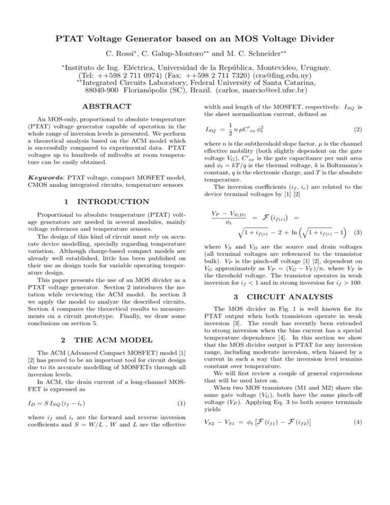
PTAT Voltage Generator based on an MOS Voltage Divider
advertisement

PTAT Voltage Generator based on an MOS Voltage Divider C. Rossi∗ , C. Galup-Montoro∗∗ and M. C. Schneider∗∗ ∗ Instituto de Ing. Eléctrica, Universidad de la República, Montevideo, Uruguay. (Tel: ++598 2 711 0974) (Fax: ++598 2 711 7320) (cra@fing.edu.uy) ∗∗ Integrated Circuits Laboratory, Federal University of Santa Catarina, 88040-900 Florianópolis (SC), Brazil. (carlos, marcio@eel.ufsc.br) ABSTRACT An MOS-only, proportional to absolute temperature (PTAT) voltage generator capable of operation in the whole range of inversion levels is presented. We perform a theoretical analysis based on the ACM model which is successfully compared to experimental data. PTAT voltages up to hundreds of milivolts at room temperature can be easily obtained. Keywords: PTAT voltage, compact MOSFET model, CMOS analog integrated circuits, temperature sensors 1 ISQ = 1 n µC 0 ox φ2t 2 (2) where n is the subthreshold slope factor, µ is the channel effective mobility (both slightly dependent on the gate voltage VG ), C 0 ox is the gate capacitance per unit area and φt = kT /q is the thermal voltage, k is Boltzmann’s constant, q is the electronic charge, and T is the absolute temperature. The inversion coefficients (if , ir ) are related to the device terminal voltages by [1] [2] INTRODUCTION Proportional to absolute temperature (PTAT) voltage generators are needed in several modules, mainly voltage references and temperature sensors. The design of this kind of circuit must rely on accurate device modelling, specially regarding temperature variation. Although charge-based compact models are already well established, little has been published on their use as design tools for variable operating temperature design. This paper presents the use of an MOS divider as a PTAT voltage generator. Section 2 introduces the notation while reviewing the ACM model. In section 3 we apply the model to analyze the described circuits. Section 4 compares the theoretical results to measurements on a circuit prototype. Finally, we draw some conclusions on section 5. 2 width and length of the MOSFET, respectively. ISQ is the sheet normalization current, defined as THE ACM MODEL The ACM (Advanced Compact MOSFET) model [1] [2] has proved to be an important tool for circuit design due to its accurate modelling of MOSFETs through all inversion levels. In ACM, the drain current of a long-channel MOSFET is expressed as ID = S ISQ (if − ir ) (1) where if and ir are the forward and reverse inversion coefficients and S = W/L , W and L are the effective ¡ ¢ VP − VS(D) = F if (r) = φt ³q ´ q 1 + if (r) − 2 + ln 1 + if (r) − 1 (3) where VS and VD are the source and drain voltages (all terminal voltages are referenced to the transistor bulk). VP is the pinch-off voltage [1] [2], dependent on VG approximately as VP = (VG − VT )/n, where VT is the threshold voltage. The transistor operates in weak inversion for if < 1 and in strong inversion for if > 100. 3 CIRCUIT ANALYSIS The MOS divider in Fig. 1 is well known for its PTAT output when both transistors operate in weak inversion [3]. The result has recently been extended to strong inversion when the bias current has a special temperature dependence [4]. In this section we show that the MOS divider output is PTAT for any inversion range, including moderate inversion, when biased by a current in such a way that the inversion level remains constant over temperature. We will first review a couple of general expressions that will be used later on. When two MOS transistors (M1 and M2) share the same gate voltage (VG ), both have the same pinch-off voltage (VP ). Applying Eq. 3 to both source terminals yields £ ¤ VS2 − VS1 = φt F (if 1 ) − F (if 2 ) (4) ID Current Mirror N ID OUT OUT ID M5 VX IN ID M1 OUT ID ID M2 (N+1) ID Start M6 M3 M4 M0 VS6 Figure 1: PTAT generating MOS divider This simple result is independent of the circuit topology as long as the gate terminals are tied together. Applying Eq. 3 to the drain and source terminals of a single MOSFET results in the following expression for its drain-source voltage: £ ¤ VDS = φt F (if ) − F (ir ) (5) 3.1 Constant Inversion Level Bias Current Generator A constant inversion level is obtained through a particular temperature dependence of the bias current which, nevertheless, is very easy to obtain with a simple circuit (Fig. 2). This topology was first proposed in [5] [6] with a limited operating range in terms of inversion coefficients. More recently it was partially extended, in a similar circuit, in [7]. In the circuit of Fig. 2, the current mirror imposes proportional currents through all branches. In order to simplify the analysis, we will consider all of them equal. As M3 and M4 share the same VG and VS , then if 3 = if 4 . Transistors M1 through M3 are saturated, so if À ir in each of them. Thus, S1 if 1 = S2 if 2 = S3 if 4 = S4 (if 4 − ir4 ) (6) Transistors M1 and M2 determine the voltage through M4 (VDS4 ) which operates in the triode region (substituting a resistor) and fixes the current through M2. The current mirror imposes a copy of this current through M1 and M3. As the elements are non-linear there is an equilibrium point which can be found by applying Eq. 4 Figure 2: MOS-only constant inversion level bias generator to M1-M2 and Eq. 5 to M4. Thus, F (if 1 ) − F (if 2 ) = F (if 4 ) − F (ir4 ) (7) The expressions in Eq. 6 and Eq. 7 are four equations that determine if 1 , if 2 , if 4 (= if 3 ) and ir4 . The inversion coefficients must be positive which imposes the condition S4 > S3 . The only parameters in the equations are the geometrical ones (S1 − S4 ), thus, the inversion coefficients are constant, independent of the temperature, and the branch currents are proportional to ISQ . Therefore, M1-M4 together with the current mirror constitute an MOS-only constant-inversion-level current generator. Some kind of start circuitry is needed to avoid the trivial solution of Eq. 7. This problem is easily solved by imposing a transient current, higher than steady-state, with an externally controlled start transistor (M0). 3.2 MOS Divider The current generator can be used to bias the MOS divider (M5 and M6) as shown in Fig. 1. Besides the main bias ID , a second (optional) current (N ID ) is included. As both transistors share the same gate voltage and the source of M5 is tied to the drain of M6, then if 5 = ir6 . M5 is saturated, so if 5 À ir5 . Thus, ID5 = ID = S5 ISQ if 5 , ID6 = (N + 1)ID = S6 ISQ (if 6 − if 5 ) (8) 0.37 0.36 0.35 chip A chip B chip C chip D theory Vx (V) 0.34 0.33 0.32 0.31 0.3 0.29 300 310 320 330 340 T (K) 350 360 370 Figure 3: Experimental and theoretical data of the PTAT voltage generator which results in if 6 = G if 5 , where · ¸ S5 G = 1 + (N + 1) S6 (9) Applying Eq. 5 to M6 and using Eq. 9 we get VX − VS6 = F (G if 5 ) − F (if 5 ) φt (10) The bias generator imposes that ID is proportional to ISQ , so (Eq. 8) if 5 is constant. As G depends only on geometrical parameters, then the right hand side of Eq. 10 is also constant, which makes VX − VS6 PTAT. If VS6 is PTAT (including the frequent case VS6 = 0), then VX is also PTAT. A closer look to the circuit should consider that ISQ exhibits some dependence on the VG of each transistor through n and µ. In the precedent analysis, all sheet normalization currents ( ISQ ) were supposed equal. Taking this effect into account makes the actual slope different than predicted. As the dependence of ISQ with VG is very weak, this variation is very slight. The sensitivity (temperature slope) of the PTAT generator can be varied by adjusting if 5 and if 6 through ID , N, S5 and S6 . In order to get a steep slope we need G À 1. If, additionally, the total current must be kept low then it usually results S6 < 1 and the circuit area increases as 1/S6 . Thus, Eq. 9 expresses a tradeoff between area and consumption. 4 EXPERIMENT The theoretical results were checked on a circuit comprising a constant inversion level bias generator and an MOS divider fabricated in a standard 0.8 µm CMOS technology. The MOS divider was designed with N = 0 while M5 was drawn as 2 µm/58 µm and M6 was implemented as the series of 24 unit transistors identical to M5. These configuration results in G = 25. The circuit was measured in a custom oven whose temperature was controlled to ±10 mK. At the lowest available temperature (305 K) the bias current was around 7 nA, thus obtaining inversion coefficient values around if 5 = 6 and if 6 = 150 corresponding, respectively, to operation in moderate and strong inversion. A combined analysis of the bias generator and the MOS divider shows that the temperature slope depends only on the geometry (S1 to S6 ). Considering typical technology values to obtain effective sizes from drawn geometries yields a 0.97 mV/K slope which is shown as a solid line in Fig. 3. This result is compared to data from the four measured chips (A to D) which are shown as dots in Fig. 3. 5 CONCLUSION We have presented a simple PTAT voltage generator based on an MOS voltage divider driven by a MOSFETonly, constant inversion level, bias current generator. The sensitivity of the PTAT voltage can be adjusted by means of both the inversion level and a current multiplication factor. PTAT voltages up to hundreds of mV at room temperature can be achieved with a MOSFET-only circuit, an interesting property not only for application as a temperature sensor but also in voltage references, for resistorless compensation of the negative temperature coefficient of bipolar transistors. Our theory is supported by experimental data from a circuit which combines transistors operating in moderate and strong inversion levels. ACKNOWLEDGEMENTS This work was partially financed by CSIC/UdelaR and Prosul/CNPq. The authors are grateful to Pablo Aguirre for his collaboration in building and operating the measurement setup. REFERENCES [1] C. Galup-Montoro, M. C. Schneider, and A. I. A. Cunha, “A current-based MOSFET model for integrated circuit design,” in Low-Voltage / LowPower Integrated Circuits and Systems: Low-Voltage Mixed-Signal Circuits, E. Sanchez-Sinencio and A. Andreou, Eds. IEEE Press, ISBN 0-7803-3446-9, 1999, ch. 2, pp. 7–55. [2] A. I. A. Cunha, M. C. Schneider, and C. GalupMontoro, “An MOS transistor model for analog circuit design,” IEEE J. Solid-State Circuits, vol. 33, no. 10, pp. 1510–1519, Oct. 1998. [3] E. A. Vittoz and O. Neyroud, “A low-voltage CMOS bandgap reference,” IEEE J. Solid-State Circuits, vol. SC-14, no. 3, pp. 573–577, June 1979. [4] C. Rossi and P. Aguirre, “Ultra−low power CMOS cells for temperature sensors,” in SBCCI 05:Proceedings of the 18th Annual Symposium on Integrated Circuits and System Design. ACM Press, Sept. 2005, pp. 202–206. [5] H. Oguey and D. Aebischer, “CMOS current reference without resistance,” in ESSCIRC 96:Proceedings of the 22nd European Solid-State Circuits Conference, Neuchâtel, Switzerland, Sept. 1996. [6] H. J. Oguey and D. Aebischer, “CMOS current reference without resistance,” IEEE J. Solid-State Circuits, vol. SC-32, no. 7, pp. 1132–1135, July 1997. [7] E. M. Camacho-Galeano, C. Galup-Montoro, and M. C. Schneider, “A 2-nW 1.1-V self-biased current reference in CMOS technology,” IEEE Trans. Circuits Syst. II, vol. 52, no. 2, pp. 61–65, Feb. 2005.


