Electrical Properties Of Nitrogen Doped Amorphous Carbon Films
advertisement
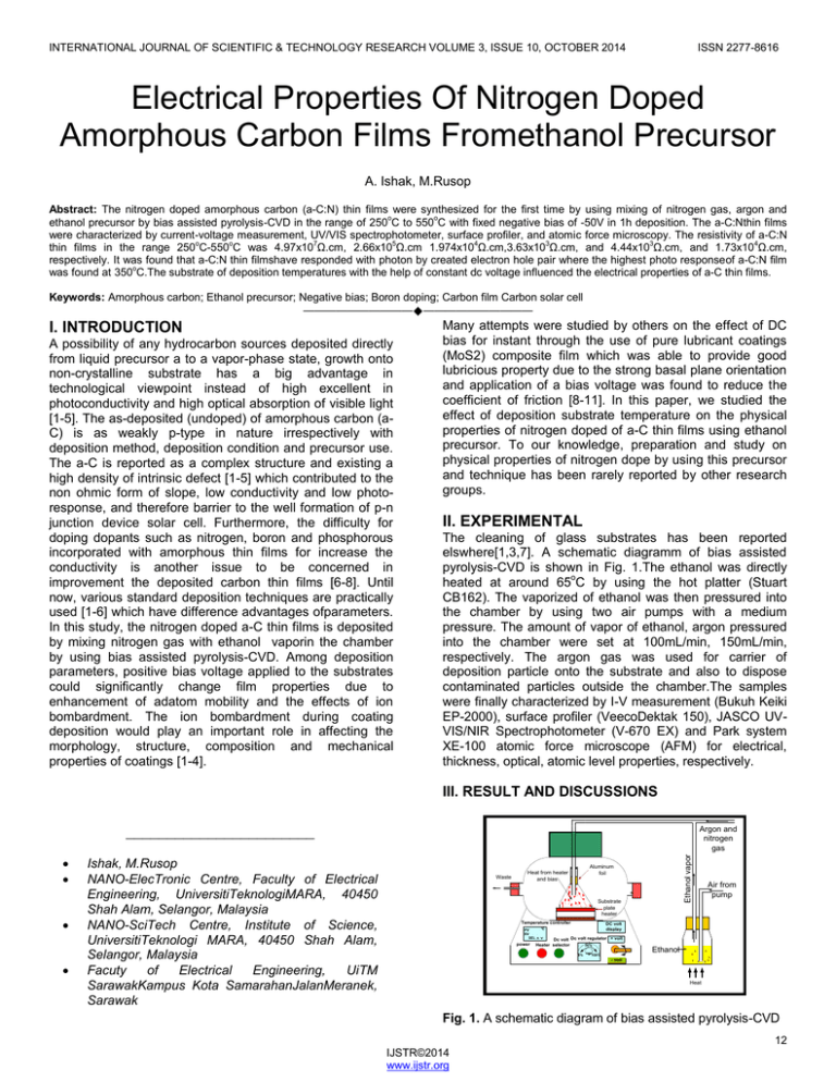
INTERNATIONAL JOURNAL OF SCIENTIFIC & TECHNOLOGY RESEARCH VOLUME 3, ISSUE 10, OCTOBER 2014 ISSN 2277-8616 Electrical Properties Of Nitrogen Doped Amorphous Carbon Films Fromethanol Precursor A. Ishak, M.Rusop Abstract: The nitrogen doped amorphous carbon (a-C:N) thin films were synthesized for the first time by using mixing of nitrogen gas, argon and ethanol precursor by bias assisted pyrolysis-CVD in the range of 250oC to 550oC with fixed negative bias of -50V in 1h deposition. The a-C:Nthin films were characterized by current-voltage measurement, UV/VIS spectrophotometer, surface profiler, and atomic force microscopy. The resistivity of a-C:N thin films in the range 250oC-550oC was 4.97x10⁷Ω.cm, 2.66x10⁵Ω.cm 1.974x10⁴Ω.cm,3.63x103Ω.cm, and 4.44x10³Ω.cm, and 1.73x10⁴Ω.cm, respectively. It was found that a-C:N thin filmshave responded with photon by created electron hole pair where the highest photo responseof a-C:N film was found at 350oC.The substrate of deposition temperatures with the help of constant dc voltage influenced the electrical properties of a-C thin films. Keywords: Amorphous carbon; Ethanol precursor; Negative bias; Boron doping; Carbon film Carbon solar cell ———————————————————— I. INTRODUCTION A possibility of any hydrocarbon sources deposited directly from liquid precursor a to a vapor-phase state, growth onto non-crystalline substrate has a big advantage in technological viewpoint instead of high excellent in photoconductivity and high optical absorption of visible light [1-5]. The as-deposited (undoped) of amorphous carbon (aC) is as weakly p-type in nature irrespectively with deposition method, deposition condition and precursor use. The a-C is reported as a complex structure and existing a high density of intrinsic defect [1-5] which contributed to the non ohmic form of slope, low conductivity and low photoresponse, and therefore barrier to the well formation of p-n junction device solar cell. Furthermore, the difficulty for doping dopants such as nitrogen, boron and phosphorous incorporated with amorphous thin films for increase the conductivity is another issue to be concerned in improvement the deposited carbon thin films [6-8]. Until now, various standard deposition techniques are practically used [1-6] which have difference advantages ofparameters. In this study, the nitrogen doped a-C thin films is deposited by mixing nitrogen gas with ethanol vaporin the chamber by using bias assisted pyrolysis-CVD. Among deposition parameters, positive bias voltage applied to the substrates could significantly change film properties due to enhancement of adatom mobility and the effects of ion bombardment. The ion bombardment during coating deposition would play an important role in affecting the morphology, structure, composition and mechanical properties of coatings [1-4]. Many attempts were studied by others on the effect of DC bias for instant through the use of pure lubricant coatings (MoS2) composite film which was able to provide good lubricious property due to the strong basal plane orientation and application of a bias voltage was found to reduce the coefficient of friction [8-11]. In this paper, we studied the effect of deposition substrate temperature on the physical properties of nitrogen doped of a-C thin films using ethanol precursor. To our knowledge, preparation and study on physical properties of nitrogen dope by using this precursor and technique has been rarely reported by other research groups. II. EXPERIMENTAL The cleaning of glass substrates has been reported elswhere[1,3,7]. A schematic diagramm of bias assisted pyrolysis-CVD is shown in Fig. 1.The ethanol was directly heated at around 65oC by using the hot platter (Stuart CB162). The vaporized of ethanol was then pressured into the chamber by using two air pumps with a medium pressure. The amount of vapor of ethanol, argon pressured into the chamber were set at 100mL/min, 150mL/min, respectively. The argon gas was used for carrier of deposition particle onto the substrate and also to dispose contaminated particles outside the chamber.The samples were finally characterized by I-V measurement (Bukuh Keiki EP-2000), surface profiler (VeecoDektak 150), JASCO UVVIS/NIR Spectrophotometer (V-670 EX) and Park system XE-100 atomic force microscope (AFM) for electrical, thickness, optical, atomic level properties, respectively. III. RESULT AND DISCUSSIONS _______________________ Ishak, M.Rusop NANO-ElecTronic Centre, Faculty of Electrical Engineering, UniversitiTeknologiMARA, 40450 Shah Alam, Selangor, Malaysia NANO-SciTech Centre, Institute of Science, UniversitiTeknologi MARA, 40450 Shah Alam, Selangor, Malaysia Facuty of Electrical Engineering, UiTM SarawakKampus Kota SamarahanJalanMeranek, Sarawak Waste Ethanol vapor Argon and nitrogen gas Aluminum foil Heat from heater and bias Substrate plate heater Temperature controller PV SV SEL power Air from pump DC volt display °C ˄˅ Dc volt Dc volt regulator + volt 50% Heater selector 0% 100% Ethanol - volt Heat Fig. 1. A schematic diagram of bias assisted pyrolysis-CVD 12 IJSTR©2014 www.ijstr.org INTERNATIONAL JOURNAL OF SCIENTIFIC & TECHNOLOGY RESEARCH VOLUME 3, ISSUE 10, OCTOBER 2014 Fig. 2 shows the current-voltage measurement of a-C:N film. An Aurum with fixed square area of approximately 0.09 cm2 is sputtered as a metal contact on a-C:N film. The resistivity and conductivity are calculated by using both equation (1) and (2) [8,9], respectively where R is the average of resistance; A is the area of metal contact and L is the length between metal two contacts. There were many forms of I-V relationships obtained in the literatures such as linear (ohmic), slightly linear, and nonlinear forms [10,11]. There is a need to form the linear behavior between current and applied voltage which is important for solar cell application. Besides the ohmic behavior, more importantly, the low resistivity and high conductivity a-C thin films as a semiconductor are required for solar cells application. + ISSN 2277-8616 The smaller slope might be due to the additional of resistance come from high density of intrinsic defects. Zeng et al [12] discussed that increasing temperature can changed the structural to form more crystallite thereby decreased the resistivity. The decreasing of the resistivity due to increasing temperatures were discussed by others [13-17]. e 0.3 cm Fig. 4 Resistivity and conductivity of a-C:N films at various deposition temperatures L Fig. 2 A Current-voltage measurement of C:N thin films on the glass substrate ρ=RA/L σ=1/ρ (1) (2) Gold as a metal contact along with semiconductor thin films was studied by many researcher [10,12]. Metals contact such as titanium (Ti), chromium (Cr), aluminum (Al) and argentum (Ag) can reacted differently with thin film[10,12]. It was found all of the slopes are in linear region when the voltage is applied from -15V to +15V. The highest slope was found at 550oC while the smallest slope contact was at 250oC. Zeng et al [12] and Liu et al [13] reported the nonlinearity was attributed to the existence and magnitude of schottky depends on the Fermi levels of semiconductor and conducting metal. Other possibility factor causedthe nonlinearity were contributed by a dielectric layer formed betweengold and semiconductor thin films. Fig. 3 Current voltage relationships of a-C:N films at various deposition temperatures Fig. 4 shows the variation resistivity and conductivity of aC:N thin films at different deposition temperature in the range of 250oC to 550oC. The resistivity of a-C:N thin films is calculated as 4.97x10⁷ Ω.cm,2.66x105 Ω.cm, 1.974x10⁴Ω.cm, 3.63x10³ Ω.cm, 4.44x10³Ω.cm, 4 4 1.85x10 Ω.cm, and 1.73x10 Ω.cm, respectively.S .M. Sze [15] summarized the resistivity range of semiconductors was in between 1x10⁸ to1x10-3 Ω.cmand by comparing with our result, we have seen that the resistivity of a-C:N thin films are semiconductor thin film We predict that, a-C:N thin films might deform structure with dopant of nitrogen to provide excess of electron thereby reduce the number of defect of thin films. Beside other factors [13,14], deposition temperature is the main role to deform the existing structure together with crystallite form. The conductivity of doped aC:N thin films is calculated by the reciprocal of resistivity values. Fig. 4shows the correlation of conductivity with changing deposition temperatures. The values of conductivity is 2.02x10⁻⁸ Scm-1, 3.76x10⁻⁶ Scm-1, 5.05x10⁻⁵ Scm-1, 5.78x10⁻⁵ Scm-1, 2.75x10⁻⁴ Scm-1, and 2.25x10⁻⁴Scm1 , respectively. The conductivity of a-C:N thin films is gradually increased by the decreasing of substrate deposition temperature 250oC to 550oC. The effect of increasing deposition temperature and doping on the increment of conductivity of thin films were also agreed and discuss by others [18-22]. A photo response is defined as the ratio of conductivity under illumination to the conductivity under dark. Table 1 shows the effect of the temperature parameters on the photo response. The values of photo response from 250oC to 550oC are 1.3722, 1.1331, 4.3779, 1.4807, 1.0271, and 1.0314, respectively. The results showed the photo response is slightly decreased from 250oC to 300oC and showed dramatically increased from 300oC to 350oC. However, at 400oC to 500oC, it was strongly decreased. We found, the highest value of photo response is at 350oC while the lowest value is at 450oC. By comparing with sloped metal contact, resistivity, conductivity, and photo response results, at 350oC is the optimum deposition temperature. Table 1 shows the influenced of temperature toward the thickness 13 IJSTR©2014 www.ijstr.org INTERNATIONAL JOURNAL OF SCIENTIFIC & TECHNOLOGY RESEARCH VOLUME 3, ISSUE 10, OCTOBER 2014 of a-C thin films. The average of thickness in the range of 250oC to 550oC is 250 nm, 230 nm, 420 nm, 103.2nm, 383.2nm, and 680nm respectively. From Table 2, the highest thickness is found at 550oC while the lowest average thickness is 230nm at 300oC. We found, the average thickness is strongly dependence with deposition temperature However, the increasing of average thicknesses was not influenced resistivity as well as conductivity. ISSN 2277-8616 The highest surface roughness is 1.842 at 250oC while the lowest surface roughness is 0.053 at 350oC. For the average grain size, 0.935 is the highest average grain size at 300oC while 0.526 is the lowest average grain size at 450oC. It is believed that grain boundary and surface roughness are directly related with the electrical properties especially carrier concentration and mobility of the electron. It was observed that both surface roughness and conductivity were decreased as the temperature was increased from 250oC to 300oC. Furthermore, the conductivity is strongly increased when the surface roughness was decreased. Similarly, the conductivity was increased as the average grain size was decreased. The effects of grain boundary and surface roughness on electrical properties were also reported by other [20-23]. AFM measurement reveals the average grain sizes for the sample at 250oC is the highest as compared with others temperatures and therefore restricts the ability for electron movement. Huang et al [23] reported thickness could also affect the conductivity. In our experiment, we found as the thickness increased, the average grain size is increased causing to decreasing the conductivity. Thisdifference in the size of the surface film can be attributed to the ion bombardment during the growth of the films which is controlled by the applied of negative bias onto the substrate. IV. CONCLUSIONS Fig.5. The AFM images of a-C thin films by in-situ doped at various temperatures AFM images of a-C:N thin films were characterized by atomic force microscopy (AFM, XE-100 Park Systems), as shown in Fig. 5 with a scan rate 1Hz and scan size of 10μm. The images show different forms of particles on the surface for all a-C:N thin films. The surface roughness from 250oC to 550oC are 1.842, 0.828, 0.053, 0.244, 0.828,and 1.448 nm while the average grain sizes are 0.802, 0.935,0.124, 0.661, 0.526, and 0.326, respectively. Table 2 The surface roughness and average grain size of a-C:N thin films in the range of 250oC-550oC Temperature (oC) Surface Roughness (nm) Average Grain Size (μm2) 250oC 1.842 0.802 300oC 0.82 0.935 350oC 0.053 0.124 400oC 0.244 0.661 450oC 0.828 0.526 550oC 1.148 0.326 The semiconducting a-C:N thin films was successfully deposited by bias assisted pyrolysis–CVD from ethanol precursor. The resistivity of a-C:N thin films deposited at 250oC to 550oC were 4.97x10⁷Ω.cm,2.66x105Ω.cm, 1.974x10⁴Ω.cm, 4.44x10³Ω.cm, 1.85x10⁴Ω.cm, and 3.63x10³ Ω.cm, respectively. Meanwhile, the conductivity of a-C thin films were 2.012x10⁻⁸ Scm-1, 3.76x10⁻⁶ Scm-1 , 5.05x10⁻⁵ Scm-1, 5.78x10⁻⁵ Scm-1, 2.75x10⁻⁴Scm-1, and 2.25x10⁻⁴ Scm-1, respectively. The resistivity was decreased as the temperature increased. The highest and the lowest photo response of a-C:N film were found at deposition temperature of 350oC, and 250oC, respectively. ACKNOWLEDGEMENT Theauthors thankto Ministry of Higher Education (MOHE) Malaysia for the scholarship, UniversitiTeknologi MARA, Kota Samarahan Sarawak and Research ManagementInstitute(RMI) UniversitiTeknologi MARA (UiTM)for thefacilities. REFERENCES [1] Ishak, K. Dayana, M. H. Mamat, M. F. Malek, and M. Rusop, Deposition of Amorphous Carbon Film Using Natural Palm Oil by Bias Assisted Pyrolysis-CVD For Solar Cell Applications, Inter. J. Power and Renew. Energy Sys. 1 (2014) 12-23. [2] S. M. Mominuzzaman, M. Rusop, T. Soga, T. Jimbo, and M. Umeno, ―Photoresponse characteristics of nitrogen doped carbon/P-silicon photovoltaic cell,‖ IEEE 4th World on Conference on Photovoltaic Energy Conversion, vol. 1, pp. 302-305, 2006. [3] A. Ishak, M. Rusop, ―Structural Properties of Micro and Nanostructured Amorphous Carbon Films from Liquid 14 IJSTR©2014 www.ijstr.org INTERNATIONAL JOURNAL OF SCIENTIFIC & TECHNOLOGY RESEARCH VOLUME 3, ISSUE 10, OCTOBER 2014 Hydrocarbon Precursor in Photovoltaic Heterojunction Solar Cell Applications‖, published in International Journal of Latest Research in Science and Technology vol. 3 (2014) pp. 90-94. [4] O. Cubero, F. j. Haug, D. Fisher, and C. Ballif, ―Reduction of the phosphorus cross-contamination in ni-p solar cells prepared in a single-chamber PECVD reactor,‖ J. Solar Energy Materials & Solar Cells, vol. 95, pp. 606-610 2011. [5] Corbell, M. Rubio-Roy, E. Bertran, and J. L. Andujar, ―Plasma parameters of pulsed-dc discharge in methane used to deposit diamondlike carbon films,‖ J. Applied Physics, vol. 106, pp. 103302-10302-11, 2009. [6] A. Mallikarjuna Reddy, A. Sivasangkar Reddy, and P. Sreedhara Reddy, ―Effect of substrate bias voltage on the physical properties of dc reactive magnetron sputtered NiO thin films,‖ J. Material Chemistry and Physics vol. 125, pp. 434-439, 2011.J. Podder, M. Rusop, T. Soga, T. Jimbo, Boron doped amorphous carbon films grown by r.f. PECVD under different partial pressure, Diamond and Related Materials 14 (2005) 1799-1804. [7] Ishak, M. Rusop, ―Structural Properties of P-Type Boron Doped Carbon Film from Hydrocarbon Palm Oil for Photovoltaic Heterojunction Solar Cell Device‖, published in International Journal of Engineering Invention vol. 3 (2014) pp. 35-41. [8] Ishak M. Amirul, and M. Rusop, ―AFM images of undoped amorphous carbon thin films deposited by bias-assisted thermal-CVD,‖ 10th International Conference on Semiconductor Electronics (ICSE2012), 2012. [9] H. Hussin, F. Mohamad, S. M. A. Hanapiah, M. Muhammad, and M. Rusop, ―Electrical properties of aC thin film deposited using methane gas as precursor,‖ International Conference on Electronic Devices, System and Aplication (ICEDSA2010), 2010.S. [10] J. Krauser, A. K. Nix, H. G. Gehrke, H. Hofsaess, C. Trautmann, and A. Weidinger, ―Conductivity enhancement of ion tracks tetrahedral amorphous carbon by doping with N, B, Cu and Fe,‖ Nuclear Instruments and Methods in Physics Research B, vol.272, pp. 280-283, 2012. ISSN 2277-8616 thin films: preparation, properties, and applications, Journal of applied Physics 54 (1983) 4590. [14] Peng Wang, Xia Wang, Youming Chen, Guangan Zhang, Weimin Liu, Junyan Zhang, The effect of applied negative bias voltage on the structure of Tidoped a-C:h films deposited by FCVA, Applied Surface Science 253 (2007) 3722-3726. [15] S.M. Sze, Semiconductor technology, Wiley 1985. devices physics and [16] F. Buebuel, I. Efeoglu, E. Arslan, The effect of bias voltage and working pressure on S/Mo ratios at MoS2Ti composite films, Applied Surface Science (2007), 253-44515-9. [17] M. Sakaki, T. Sakakibara, Ionization and reaction mechanism of a reactive cathodic arc deposition of TiN. IEEE Trans Plasma Science (1994) 22. [18] M. S. Leu, S. Y. Chen, J. J. Chang,, et al. Diamond-like coatings prepared by the filtered cathodic arc technique for minting application, Surface Coating Technology 177-178 (2004) 566. [19] Dwivedi, Neeraj Kumar, Sushil Malik, and K. Hitendra, ―Studied on pure and nitrogen-incorporated hydrogenated amorphous carbon thin films and their possible application for amorphous silicon solar cells,‖ Journal of Applied Physics, vol. 111, pp. 14908-14916, Jan. 2012. [20] R. Gharbi, M. Fathallah, N. Alzaied, E. Tresso, and A. Tagliaferro, ―Hydrogen and nitrogen effects on optical and structural properties of amorphous carbon,‖ Mater. Sci. Eng. C, vol. 28, pp. 795, 2008 . [21] L. Y. Huang, L. Meng, ―Effects of films thickness on microstructure and electrical properties of the pyrite films, ― Mater. Sci. Eng. B, vol. 137, pp. 310, 2007. [22] E. Liu, L. Li, B. Blainpain, Residual stresses of diamond and diamondlike carbon films, Journal of Applied Physics, 98 (2005) 073515. [23] Hiroki Akasaka, Takatoshi Yamada, and Naoto Ohtake, ―Effect of film structure on field emission properties of nitrogen doped hydrogenated amorphous carbon films,‖ Journal In Diamond & Related Materials, vol. 18, pp. 423-425, 2009. [11] F.M. Wang, M.W. Chen, and Q.B. Lai, ―Mettalic contacts to nitrogen and boron doped diamond-like carbon films,‖ Thin Solid Films, vol. 518, pp. 33323336, 2010. [12] A.P. Zeng, Y.B. Yin, M. Bilek, and D. McKenzie, ―Ohmic contact to nitrogen doped amorphous carbons films,‖ Surface Coating Technology 198 (2005) 202. [13] A. Bubenzer, B. Dischler, G. Brandt, P. Koids, rfplasma deposited amorphous hydrgenated hard carbon 15 IJSTR©2014 www.ijstr.org
