High-performance organic thin-film transistors with metal oxide
advertisement
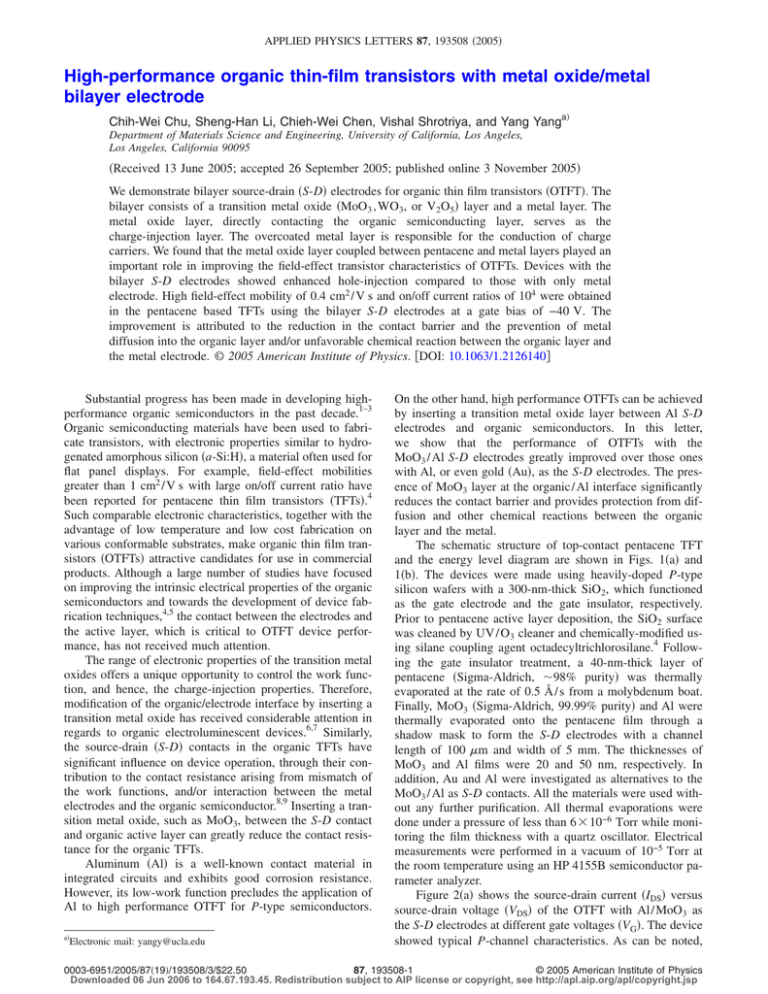
APPLIED PHYSICS LETTERS 87, 193508 共2005兲 High-performance organic thin-film transistors with metal oxide/metal bilayer electrode Chih-Wei Chu, Sheng-Han Li, Chieh-Wei Chen, Vishal Shrotriya, and Yang Yanga兲 Department of Materials Science and Engineering, University of California, Los Angeles, Los Angeles, California 90095 共Received 13 June 2005; accepted 26 September 2005; published online 3 November 2005兲 We demonstrate bilayer source-drain 共S-D兲 electrodes for organic thin film transistors 共OTFT兲. The bilayer consists of a transition metal oxide 共MoO3 , WO3, or V2O5兲 layer and a metal layer. The metal oxide layer, directly contacting the organic semiconducting layer, serves as the charge-injection layer. The overcoated metal layer is responsible for the conduction of charge carriers. We found that the metal oxide layer coupled between pentacene and metal layers played an important role in improving the field-effect transistor characteristics of OTFTs. Devices with the bilayer S-D electrodes showed enhanced hole-injection compared to those with only metal electrode. High field-effect mobility of 0.4 cm2 / V s and on/off current ratios of 104 were obtained in the pentacene based TFTs using the bilayer S-D electrodes at a gate bias of −40 V. The improvement is attributed to the reduction in the contact barrier and the prevention of metal diffusion into the organic layer and/or unfavorable chemical reaction between the organic layer and the metal electrode. © 2005 American Institute of Physics. 关DOI: 10.1063/1.2126140兴 Substantial progress has been made in developing highperformance organic semiconductors in the past decade.1–3 Organic semiconducting materials have been used to fabricate transistors, with electronic properties similar to hydrogenated amorphous silicon 共a-Si:H兲, a material often used for flat panel displays. For example, field-effect mobilities greater than 1 cm2 / V s with large on/off current ratio have been reported for pentacene thin film transistors 共TFTs兲.4 Such comparable electronic characteristics, together with the advantage of low temperature and low cost fabrication on various conformable substrates, make organic thin film transistors 共OTFTs兲 attractive candidates for use in commercial products. Although a large number of studies have focused on improving the intrinsic electrical properties of the organic semiconductors and towards the development of device fabrication techniques,4,5 the contact between the electrodes and the active layer, which is critical to OTFT device performance, has not received much attention. The range of electronic properties of the transition metal oxides offers a unique opportunity to control the work function, and hence, the charge-injection properties. Therefore, modification of the organic/electrode interface by inserting a transition metal oxide has received considerable attention in regards to organic electroluminescent devices.6,7 Similarly, the source-drain 共S-D兲 contacts in the organic TFTs have significant influence on device operation, through their contribution to the contact resistance arising from mismatch of the work functions, and/or interaction between the metal electrodes and the organic semiconductor.8,9 Inserting a transition metal oxide, such as MoO3, between the S-D contact and organic active layer can greatly reduce the contact resistance for the organic TFTs. Aluminum 共Al兲 is a well-known contact material in integrated circuits and exhibits good corrosion resistance. However, its low-work function precludes the application of Al to high performance OTFT for P-type semiconductors. a兲 Electronic mail: yangy@ucla.edu On the other hand, high performance OTFTs can be achieved by inserting a transition metal oxide layer between Al S-D electrodes and organic semiconductors. In this letter, we show that the performance of OTFTs with the MoO3 / Al S-D electrodes greatly improved over those ones with Al, or even gold 共Au兲, as the S-D electrodes. The presence of MoO3 layer at the organic/ Al interface significantly reduces the contact barrier and provides protection from diffusion and other chemical reactions between the organic layer and the metal. The schematic structure of top-contact pentacene TFT and the energy level diagram are shown in Figs. 1共a兲 and 1共b兲. The devices were made using heavily-doped P-type silicon wafers with a 300-nm-thick SiO2, which functioned as the gate electrode and the gate insulator, respectively. Prior to pentacene active layer deposition, the SiO2 surface was cleaned by UV / O3 cleaner and chemically-modified using silane coupling agent octadecyltrichlorosilane.4 Following the gate insulator treatment, a 40-nm-thick layer of pentacene 共Sigma-Aldrich, ⬃98% purity兲 was thermally evaporated at the rate of 0.5 Å / s from a molybdenum boat. Finally, MoO3 共Sigma-Aldrich, 99.99% purity兲 and Al were thermally evaporated onto the pentacene film through a shadow mask to form the S-D electrodes with a channel length of 100 m and width of 5 mm. The thicknesses of MoO3 and Al films were 20 and 50 nm, respectively. In addition, Au and Al were investigated as alternatives to the MoO3 / Al as S-D contacts. All the materials were used without any further purification. All thermal evaporations were done under a pressure of less than 6 ⫻ 10−6 Torr while monitoring the film thickness with a quartz oscillator. Electrical measurements were performed in a vacuum of 10−5 Torr at the room temperature using an HP 4155B semiconductor parameter analyzer. Figure 2共a兲 shows the source-drain current 共IDS兲 versus source-drain voltage 共VDS兲 of the OTFT with Al/ MoO3 as the S-D electrodes at different gate voltages 共VG兲. The device showed typical P-channel characteristics. As can be noted, 0003-6951/2005/87共19兲/193508/3/$22.50 87, 193508-1 © 2005 American Institute of Physics Downloaded 06 Jun 2006 to 164.67.193.45. Redistribution subject to AIP license or copyright, see http://apl.aip.org/apl/copyright.jsp 193508-2 Chu et al. Appl. Phys. Lett. 87, 193508 共2005兲 FIG. 1. 共a兲 Structure of the organic thin film transistor; 共b兲 energy level diagrams of pentacene, MoO3 and the metals 共Al, Au兲. the output characteristics displayed very good, clear saturation currents which behaved quadratically as a function of the gate bias. The corresponding plots of −IDS and 共−IDS兲1/2 versus VG for the device are shown in Fig. 2共b兲. Strong fieldeffect modulation of the channel conductance was observed, with on/off current ratios 共Ion / Ioff兲 as high as 104 共measured between gate voltage, VG = −40–10兲. The field-effect mobility 共兲 was calculated at the saturation regions from the following equation:10 IDS = 共WCi/2L兲共VG − VT兲2 , where Ci is the capacitance per unit area of the insulator, and VT is the threshold voltage. The field-effect mobility and the threshold voltage of the OTFT were 0.40 cm2 / V s and −10.43 V, respectively. On the other hand, Figs. 3共a兲 and 3共b兲 show IDS versus VDS curves for the OTFTs with Au and Al as the S-D electrodes, respectively. Both these devices showed typical P-channel characteristics as well. The transfer characteristics for different materials for the S-D electrodes are shown in Figs. 4共a兲 and 4共b兲. The device with Au S-D electrode had similar Ion / I0ff compared to the device with MoO3 / Al S-D electrode, while Ion / Ioff for the Al electrode was 102. In addition, the decreased slope of the transfer characteristics corresponded to a twofold decrease in the field-effect mobility to h = 0.18 cm2 / V s for the Au contacts. For the case of Al, the saturation current of the channel further reduced, and field-effect mobility of 2.8 ⫻ 10−3 cm2 / V s was calculated. These results demonstrate that the introduction of the metal oxide in our OTFTs played an important role in decreasing the contact resistance. Other metal oxides were combined with Al for the S-D electrodes and the electrical characteristics of the OTFTs with different S-D electrodes in this study are summarized in Table I. In order to understand the performance improvement in the devices with MoO3 / Al as electrodes, we must consider the electronic properties of the transition metal oxide. The FIG. 2. 共a兲 Source-drain current-voltage characteristics of the OTFT with MoO3 / Al electrodes. 共b兲 The transfer characteristics of the OTFT with MoO3 / Al electrodes at a constant drain voltage of −40 V. energy level diagrams for pentacene, MoO3, Au, and Al are illustrated in Fig. 1共b兲. MoO3 is a wide gap semiconductor with band gap of 3–3.1 eV, and an electron affinity of around 2.2 eV,11,12 which implies the valance band position at around 5.3 eV. The highest occupied molecular orbital 共HOMO兲 of pentacene lies at 5.0 eV 共Ref. 13兲 and is aligned with the valence band of MoO3, resulting in no barrier for injection of holes into the pentacene layer. It has been suggested that the excess constituent can act as doping centers FIG. 3. Source-drain current-voltage characteristics of the OTFT where the source-drain electrodes are: 共a兲 Au and 共b兲 Al. Downloaded 06 Jun 2006 to 164.67.193.45. Redistribution subject to AIP license or copyright, see http://apl.aip.org/apl/copyright.jsp 193508-3 Appl. Phys. Lett. 87, 193508 共2005兲 Chu et al. FIG. 4. Transfer characteristics for different materials as the source-drain contacts MoO3 / Al 共䊏兲; Au 共쎲兲; Al 共䉱兲: 共a兲 −ISD − VG and 共b兲 共−ISD兲1/2 − VG plots at VD = −40 V. and that this dopant controls the electrical properties of the film.14,15 Since MoO3 layer was deposited by evaporation, MoO3 yields a film containing species from MoO to MoO3 as well as free Mo. Additionally, impurities might be introduced into the film, arising from boats used during thermal evaporation, as well as from the impurities present in MoO3 powder. The width of the depletion region between metal and MoO3 junction decreases as the doping concentration in the MoO3 film increases; as a result, the probability of tunneling through the barrier increases. Therefore, an Ohmic contact is likely to be achieved at the metal and MoO3 interface. To further demonstrate this, devices were fabricated using MoO3 covered with different metals 共Au, Ag, and Al兲 as the electrodes. Figure 5 shows the transfer characteristics of OTFTs using MoO3 covered with different metals as the electrodes. They show similar electrical characteristics and improved performance compared to metal-only electrodes. Because of the small mismatch between the work function of Au and the HOMO level of pentacene, Au is one of the most promising metal electrodes for pentacene TFTs. However, metals deposited onto the pentacene surface either penetrate the surface, thereby doping the upper layer of pentacene, or diffuse into pentacene to form a metallic overlayer, which is a mixture of metal and pentacene instead of pure metal. The interface dipole immediately forms increasing the barrier height between metal and pentacene.16 The modified MoO3 layer interface provides protection against metal diffusion into the organic layer and an unfavorable chemical reaction between organic and metal electrodes. The modifiTABLE I. Electrical parameters of the OTFTs in this study. Drain-source electrodes Mobility 共cm2 / V s兲 Threshold voltage 共V兲 On-off ratio Al Au MoO3 / Al WO3 / Al V2O5 / Al 2.8⫻ 10−3 0.182 0.4 0.253 0.226 −16.2 −8.75 −12.1 −12.88 −10.43 2.3⫻ 102 2.8⫻ 104 3.8⫻ 104 4.1⫻ 104 1.8⫻ 104 FIG. 5. Transfer characteristics 共−ISD vs VG兲 of OTFTs using MoO3 covered with different metals as the electrodes. MoO3 / Au 共쎲兲; MoO3 / Ag 共䊏兲; MoO3 / Al 共䉱兲. cation decreases the intensity of interface dipole and enhances charge injection. In conclusion, the OTFTs with MoO3 as a hole injection layer between the metal electrodes and the organic semiconductor layer were fabricated through thermal evaporation. Compared with OTFTs without the metal oxide, the current and the field-effect mobility were significantly improved. Therefore, using a transition metal oxide as the hole injection layer is an effective way to improve the characteristics of OTFTs, making the device suitable for commercial applications. Financial support from the Air Force of Scientific Research 共Program manager Dr. Charles Lee, Grant No. F49620-03-1-0101兲 is deeply appreciated. C.W.C is also grateful for the financial support from MediaTek Fellowship. C. W. Tang and S. Van Slyke, Appl. Phys. Lett. 51, 913 共1987兲. P. Peumans, A. Yakimov, and S. R. Forrest, J. Appl. Phys. 93, 3693 共2003兲. 3 H. E. Katz and Z. Bao, J. Phys. Chem. B 104, 671 共2000兲. 4 Y. Lin, D. J. Gundlach, S. F. Nelson, and T. N. Jackson, IEEE Trans. Electron Devices 18, 606 共1997兲. 5 M. Shtein, J. Mapei, J. B. Benziger, and S. R. Forrest, Appl. Phys. Lett. 81, 268 共2002兲. 6 J. Kido, T. Matsumoto, T. Nakada, J. Endo, K. Mori, N. Kawamura, and A. Yoko, SID Int. Symp. Digest Tech. Papers 34, 964 共2003兲. 7 G. L. Frey, K. J. Reynolds, and R. H. Friend, Adv. Mater. 共Weinheim, Ger.兲 14, 265 共2002兲. 8 R. Hajlaoui, G. Horowitz, F. Garnier, A. Arce-Brouchet, L. Laigre, A. El Kassmi, F. Demanze, and F. Kouki, Adv. Mater. 共Weinheim, Ger.兲 9, 389 共1997兲. 9 C. Waldauf, P. Schilinsky, M. Perisutti, J. Hauch, and C. J. Brabec, Adv. Mater. 共Weinheim, Ger.兲 15, 2084 共2003兲. 10 S. M. Sze, Physics of Semiconductor Devices 共Wiley, New York, 1981兲. 11 T. Yasuda, T. Goto, K. Fujita, and T. Tsutsui, Appl. Phys. Lett. 85, 2098 共2004兲. 12 P. A. Cox, Transition Metal Oxides, An Introduction to Their Electronic Structure and Properties 共Clarendon, Oxford, 1992兲. 13 A. Galtayries, S. Wisniewski, and J. Grimblot, J. Electron Spectrosc. Relat. Phenom. 87, 31 共1997兲. 14 J. G. Simmons, Phys. Rev. 166, 912 共1968兲. 15 G. S. Nadkarni and J. G. Simmons, J. Appl. Phys. 41, 545 共1970兲. 16 N. J. Watkins, L. Yan, and Y. L Gao, Appl. Phys. Lett. 80, 4384 共2002兲. 1 2 Downloaded 06 Jun 2006 to 164.67.193.45. Redistribution subject to AIP license or copyright, see http://apl.aip.org/apl/copyright.jsp
