high power factor induction heating system with
advertisement

International Journal of Electrical, Electronics and Mechanical Controls
ISSN (Online) : 2319-7501
Volume 4 Issue 2 May 2015
Manuscript ID : ISSN23197501-V4I2M2-052015
HIGH POWER FACTOR INDUCTION HEATING SYSTEM
WITH INTERLEAVED VARIABLE DUTY CYCLE
S.Ravikanth 1
1
V.Hanuma Naik 2
Assistant Professor, Sarojini Institute of Technology, Telaprolu, Vijayawada, Krishna Dt, A.P, India
Assistant Professor, Sarojini Institute of Technology, Telaprolu, Vijayawada, Krishna Dt, A.P, India
2
Abstract- This project presents the analysis and design of
a new ac–ac resonant converter applied to domestic
induction heating. The proposed topology, based on the
half-bridge series resonant inverter, uses only two diodes
to rectify the mains voltage. The proposed converter can
operate with zero-voltage switching during both switch-on
and switch-off transitions. This modified topology and
interleaved pulsing gives a nearly unity power factor. As a
consequence, the converter efficiency is significantly
improved. The analytical and simulation results have
been verified by means of a 3600-W induction heating
prototype. An efficiency study has been carried out,
obtaining values higher than 96%.
Keywords-component; ac–ac resonant converter, zerovoltage switching
I. INTRODUCTION
INDUCTION heating appliance market is
increasing due to its fastest heating time and
efficiency. Domestic induction hobs are now
becoming a standard option, especially in Asia and
Europe. The principle of operation is based on the
generation of a variable magnetic field by means of a
planar inductor below a metallic vessel [1], [2]. The
mains voltage is rectified and after that an inverter
provides a medium-frequency current to feed the
inductor. The usual operating frequency is higher
than 20 kHz to avoid the audible range and lower
than 100 kHz to reduce switching losses. The most
used device is the insulated gate bipolar transistor
(IGBT) because of the operating frequency range and
the output power range, up to 3 kW. Nowadays, most
Designs use the half-bridge series resonant topology
because of its control simplicity and high efficiency
[3]–[7]. In the past, several ac–ac topologies have
been proposed to simplify the converter and improve
the efficiency [8]–[10]. Considering the induction
Heating application, several resonant matrix
converters featuring MOSFETs [11], [12], IGBTs
[13], or RB-IGBTs [14], [15] have been proposed.
However,
the
final
efficiency and cost are compromised due to the use of
International Journal of Electrical, Electronics and Mechanical Controls
ISSN (Online) : 2319-7501
Volume 4 Issue 2 May 2015
Manuscript ID : ISSN23197501-V4I2M2-052015
a higher number of switching devices. Other
approaches, commonly used in electronic ballasts,
simplify the rectifier stage in order to improve the
converter performance [16]–[21]. This topology,
known as half-bridge boost rectifier, reduces the
switch count while keeping the same performance as
more complex solutions. The aim of this paper is to
propose a new topology to improve the efficiency
while reducing the power device count for induction
heating applications. The proposed topology is based
on the series resonant half-bridge topology and
requires only two rectifier diodes. The effective
output voltage is doubled, as in [22], [23], allowing a
significant current reduction in the switching devices.
Moreover, the proposed topology can operate with
zero-voltage switching conditions during turn-on for
both switching devices, and also during turn-off
transitions for one of them. As a consequence, the
efficiency is improved while the device count is
reduced. This paper is organized as follows. Section
II describes the proposed topology. In Section III, a
deeper analysis of the power converter is performed.
Sections IV and V show the main simulation and
experimental results, respectively. Finally, Section VI
draws the main conclusions of this paper.
II. PROPOSED POWER CONVERTER
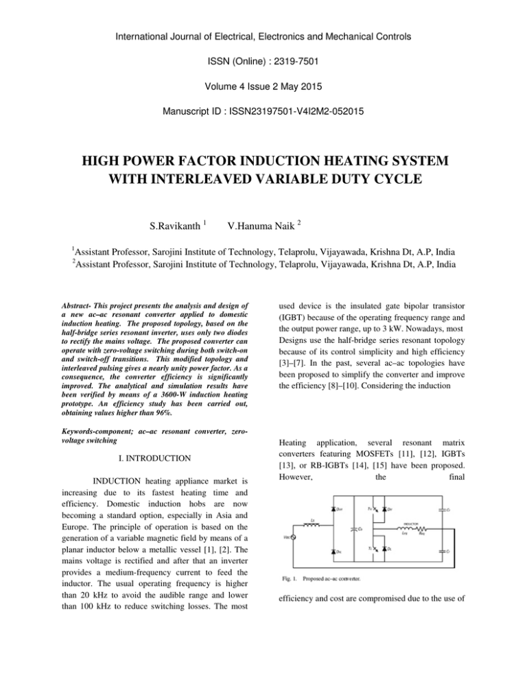
The proposed topology (see Fig. 1) employs
two bidirectional switches SH and SL composed of a
transistor TH or TL , typically an IGBT, and an ant
parallel diode DH or DL , respectively. The mains
voltage vac is rectified by two diodes DrH and DrL,
but only one of them is activated at the same time.
This operation increases efficiency with regard to
classical topologies based on a full-bridge diode
rectifier plus a dc-link inverter. The proposed
topology is a series–parallel resonant converter. The
inductor–pot system is modeled as an equivalent
series resistance Req and inductance Leq, as shown.
This topology implements resonant capacitors Cr and
may use a bus capacitor Cb. Due to the symmetry
between positive and negative mains voltage, both
resonant capacitors have the same value. An input
inductor Ls is used to reduce the harmonic content to
fulfill the electromagnetic compatibility regulations.
III. ANALYSIS
The topology presents symmetry between positive
and negative ac voltage supply. Its symmetry
simplifies analysis and makes possible to redraw the
circuit as shown in Fig. 2. Although this topology
uses different resonant configurations, parallel and
series, and different resonant tanks for each of them,
it is possible to use a normalized nomenclature based
on series resonance
Where α is the ratio between the dc-link and the
resonant capacitors and β is the ratio between the
input choke and the equivalent inductance of the
inductor–pot system. The parameters {ω0, ωsw, ωn}
are the angular resonant frequency, the angular
switching frequency, and the normalized angular
International Journal of Electrical, Electronics and Mechanical Controls
ISSN (Online) : 2319-7501
Volume 4 Issue 2 May 2015
Manuscript ID : ISSN23197501-V4I2M2-052015
switching frequency, respectively. Z0 defines the
equivalent impedance of the resonant circuit, defined
by Leq and Cr. Finally, Qeq is the equivalent
inductor–pot system quality factor at the resonant
frequency. The system will be analyzed using the
state-space description. Each state is completely
defined by a differential equation system and the
global system response is the conduction angle, θ,
average
response
of
each
state
(I–III):
where the state variables x = [is, vCb, vCrH, vCrL, i0
]T are the input current, the voltage across the bus
capacitor Cb, the voltage across both resonant
capacitors, and the current through the load,
respectively. As is shown in Fig. 3, working under
ZVS conditions, there are three different states. Each
one has its characteristic differential equation system.
Fig. 4 shows the transition conditions for each state.
State I operate with the high-side switching device
SH triggered-on and activated and the low-side
switching device (SL) triggered-off. The parallel
resonant circuit is set by an equivalent capacitor Ceq
, obtained from Cr and Cb and expressed in (8), and
the inductor electrical parameters, Req and Leq . The
current flowing through SH is the same as the one
flowing
through
the
load
State I begins when SL is triggered OFF. In this
moment, the anti parallel diode DH conducts and SH
can be triggered ON ensuring ZVS switching-on
conditions. Transitions from this state can lead either
to state II or state III. If voltage across SL reaches
zero and DL starts conducting, the transition
condition to state II is fulfilled. On the other hand, if
SH is switched OFF when TH conducts, the next state
is state III. The normalized differential equations that
define the dynamics of the system in this state are
State II is characterized by the conduction of both
switching devices, although only SH is triggered ON.
That is, TH and DL conduct at the same time. Current
through load is supplied by both devices (TH and DL
), and consequently, low conduction stress for the
devices is achieved. The equivalent parallel resonant
circuit is set by the inductor electrical parameters in
parallel with both resonant capacitors. Cb is shortcircuited by both switching devices. This state starts
when the voltage across SL reaches zero. At this
moment, DL starts conducting at the same time as TH
is triggered ON. This state finishes when SH is
triggered OFF and the next state is state III. The main
benefit results of the lower switch-off current
achieved when SH is triggered OFF, due to the fact
that the load current is supplied by both devices. In
addition, SH achieves ZVS conditions during both
switches-on and switch-off transitions, reducing
consequently the switching losses. The normalized
differential equati State III is defined by the
International Journal of Electrical, Electronics and Mechanical Controls
ISSN (Online) : 2319-7501
Volume 4 Issue 2 May 2015
Manuscript ID : ISSN23197501-V4I2M2-052015
conduction of SL while SH is deactivated. The
equivalent resonant circuit is set by one resonant
capacitor in parallel with the series connection of the
Cb capacitor and the parallel connection of the
inductor and the other one resonant capacitance. Note
that when Cb is zero (α = 0), the equivalent resonant
circuit is a series RLC circuit composed of the
inductor–pot system and one resonant capacitor. This
state starts when SH is triggered OFF. At this
moment, DL starts conducting and SL can be
triggered ON achieving ZVS switch-on conditions.
This state finishes when SL is deactivated, and the
next state is state I.
IV. SIMULATION RESULTS
By using the space-state analysis presented in Section
III, two operating modes can be described (see Fig.
5). Both of them achieve ZVS switch-on conditions;
however, only the first operation mode can achieve
the ZVS switch-off conditions for SH . The first
operation mode uses the three states described earlier:
I, II, and III. It makes possible to achieve ZVS
conditions for the high-side switch in state II. The
low-side switch has non- ZVS turn-off characteristic.
However, turn-off current is always lower than in the
high-side switch. The second operation mode only
uses two states: I and III. This operation mode does
not achieve ZVS conditions during switch-off, and
the switching losses are, therefore, increased. This
switching loss can be reduced by using snubber
capacitors [25], [26]. Nowadays, the induction
heating appliances’ power is limited by mains
maximum current and voltage. The typical maximum
output power is 3600W, and the power converter
prototype has been, therefore, designed to achieve
3600-W output power. Simulation parameters are Cr
= 470 nF, and the inductor is modeled by Leq = 65
µH and 6.5 Ω for the series-equivalent resistor at
switching frequency. The dc-link capacitor has been
selected to be low enough to obtain a high power
factor and a proper power control, as it is shown in
this section, and it can be neglected in this analysis.
The control strategies considered to control the
output power are the square wave (SW) control,
based on changing the switching frequency, and the
asymmetrical duty cycle control [6], [25], [27], based
on changing the duty cycle of the switching devices.
Next subsections detail the main simulation results.
A. SW Control Review Stage
The SW control modifies the output power by
controlling the switching frequency. The switching
frequency is higher than the resonant frequency to
achieve switch-on ZVS, and the output power is
reduced when the switching frequency is increased
(see Fig. 6). As is shown in Fig. 6, the frequency
range starts at 22 kHz, which is the resonant
frequency determined by Leq and Cr , that ensures
ZVS switching-on conditions, and can be increased
to decrease the output power. However, if the
switching frequency reaches 30 kHz, switching-off
losses increase because ZVS switching-off conditions
are not achieved. As a result, the suitable switching
frequency range and, therefore, the output power
range is reduced. To overcome this limitation, the
asymmetric duty cycle (ADC) control strategy is
proposed.
B. Asymmetrical Duty Cycle Control
The ADC control varies the output power by
changing the switching device duty cycle. As is
shown in Fig. 7, this control strategy delivers
different output powers by changing the percent of
conducting angle (θ) in which the high-side switch
SH is activated D(SH ). The low-side switch SL
conducting angle can be calculated as follows:
where θ DT is the dead-time conducting angle to
avoid short circuits. The variation of conducting
angle is restricted by the achievement of softswitching conditions for SH, ZVS for switching-off,
and by the achievement of ZVS in the switching on
commutation for both devices (anti parallel diode
conduction at the beginning). In order to operate with
switch-on ZVS conditions, the duty cycle must be
higher than 30%. The upper boundary is kept to 60%
to obtain a proper safety margin and balance the total
amount of losses per switching device. Fig. 8 shows
International Journal of Electrical, Electronics and Mechanical Controls
ISSN (Online) : 2319-7501
Volume 4 Issue 2 May 2015
Manuscript ID : ISSN23197501-V4I2M2-052015
the power output variation achieved and the
switching losses.
One of the key design aspects when designing the
proposed converter to operate with the ADC control
is the voltage that the switching devices must
withstand. Fig. 9 shows the value of the voltage
normalized to the input mains voltage as a function of
the duty cycle for loads with (a) different Q eq and
(b)different
bus capacitors for the same Q eq . In this figure, the
optimum switching area is plotted with the solid line.
As is shown in Fig. 9(a), the induction load must be
carefully designed to avoid unfeasible high voltages.
Besides, Fig. 9(b) shows that the bus capacitor
significantly
reduces
the
duty
cycle
operating range, whereas the voltage in the switching
device is reduced. As a conclusion, for this design the
bus capacitor is removed to improve the duty cycle
operating range and, consequently, the output power
control, and to reduce the number of components.
However, other designs with lower output power
control requirements may benefit of the voltage
reduction.
As a conclusion, the output power in the proposed
converter can be effectively controlled by means of
International Journal of Electrical, Electronics and Mechanical Controls
ISSN (Online) : 2319-7501
Volume 4 Issue 2 May 2015
Manuscript ID : ISSN23197501-V4I2M2-052015
SW and ADC control strategies. The output power
can be reduced from the maximum value at the
resonant frequency, 3000W, to 1000Wwithout
degrading the converter efficiency. If further
reduction is required, pulse density modulation
(PDM) [28] can be used to keep a high efficiency.
The next section shows the main experimental results
to validate the analytical and simulation results.
V. CONCLUSION
The previous papers had studied, and it is planned to
implement power factor correctioin. It is planned to
simulate using matlab 7.10. and hardware block
diagram has been designed. The project describing a
low cost solution is realized to the problem of
controlling the operation of a resonant inverter
designed for an induction cooker. It is very clear that
operating at high frequencies in the order of 25 khz
gives a better Dc voltage to the inverter circuit. More
over the effficienc of the system is fine when it is
operated at 25 khz. The output power is about 4.8kw.
The symmetricity in the output voltage and current is
obtained at high switching frequencies. The
controller permits both the control of the output
power level of the cooker and assures a nearly unity
power factor sinusoidal current to be drawn from the
mains side. The procedure is applied to the induction
cooker system and the design steps and test results
are presented.
REFERENCES
[1] J.Acero, J. M. Burdio, L.A. Barragan, D. Navarro,
R.Alonso, J. R. Garcia, F. Monterde, P. Hernandez,
S. Llorente, and I. Garde, “Domestic induction
appliances,” IEEE Ind. Appl. Mag., vol. 16, no. 2, pp.
39–47, Mar./Apr. 2010.
[2] H. Fujita, N. Uchida, and K. Ozaki, “A new zonecontrol induction heating system using multiple
inverter units applicable under mutual magnetic
coupling conditions,” IEEE Trans. Power Electron.,
vol. 26, no. 7, pp. 2009–2017, Jul. 2010.
[3] I. Mill´an, J. M. Burd´ıo, J. Acero, O. Luc´ıa, and
S. Llorente, “Series resonant inverter with selective
harmonic operation applied to all-metal domestic
induction heating,” IET Power Electron., vol. 4, pp.
587–592, May 2011.
[4] R. L. Steigerwald, “A comparison of half-bridge
resonant converter topologies,” IEEE Trans. Power
Electron., vol. 3, no. 2, pp. 174–182, Apr. 1988.
[5] H. W. Koertzen, J. D. van Wyk, and J. A.
Ferreira, “Design of the halfbridge series resonant
converters for induction cooking,” in Proc. IEEE
Power Electron. Spec. Conf. Records, 1995, pp. 729–
735.
[6] H. Pham, H. Fujita, K. Ozaki, and N. Uchida,
“Phase angle control of high-frequency resonant
currents in a multiple inverter system for zonecontrol
induction heating,” IEEE Trans. Power Electron.,
vol. 26, no. 11, pp. 3357–3366, Nov. 2011.
[7] W. Yunxiang, M. A. Shafi, A. M. Knight, and R.
A. McMahon, “Comparison of the effects of
continuous and discontinuous PWM schemes on
power losses of voltage-sourced inverters for
induction motor drives,”
IEEE Trans. Power Electron., vol. 26, no. 1, pp. 182–
191, Jan. 2011.
First Author: S.Ravikanth, graduate in
electrical and electronics engineering (EEE) from Prasad Institute
Of Technology and Sciences, Jaggayyapet,& his M.Tech from
Nalanda Institute of Engineering and Technology, Kantepudi,
Sattenapalli, Guntur Dist.,A.P,India,He is working as Assistant
Professor in Dep. Of EEE at, Sarojini Institute of Technology,
Telaprolu,
Vijayawada,
Krishna
Dt,
A.P,
India
,
Vijayawad.Affliated toJNTUK, Kakinada, A.P, India His Research
Interests are Power Systems, Power Electronics and drives, Non
Conventional Energy Sources & FACTS devices.
International Journal of Electrical, Electronics and Mechanical Controls
ISSN (Online) : 2319-7501
Volume 4 Issue 2 May 2015
Manuscript ID : ISSN23197501-V4I2M2-052015
Second Author: V.Hanuma Naik,
graduate in electrical and electronics engineering (EEE) from Sri
Chundi Ranganayakula engineering college, chilakaluripet,Guntur
dt & his M.Tech from National Institute of Technology Calicut
Kerala, India, He is working as Assistant Professor & Head Of
The Department in Dep. Of EEE at, Sarojini Institute of
Technology, Telaprolu, Vijayawada, Krishna Dt, A.P, India,
Vijayawada.Affliated to JNTUK, Kakinada, A.P, and India His
Research Interests are Power Systems, Electrical machines,
Electrical measurements & FACTS devices.


