MWR-0565 REPRINT.indd
advertisement

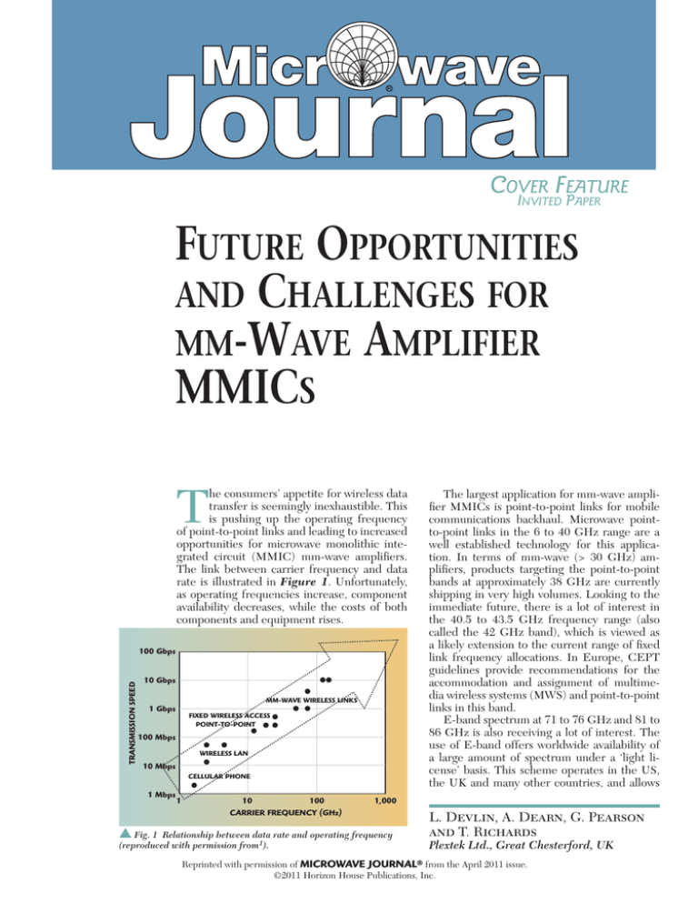
Cover Feature Invited Paper Future Opportunities and Challenges for mm-Wave Amplifier MMICs T he consumers’ appetite for wireless data transfer is seemingly inexhaustible. This is pushing up the operating frequency of point-to-point links and leading to increased opportunities for microwave monolithic integrated circuit (MMIC) mm-wave amplifiers. The link between carrier frequency and data rate is illustrated in Figure 1. Unfortunately, as operating frequencies increase, component availability decreases, while the costs of both components and equipment rises. TRANSMISSION SPEED 100 Gbps 10 Gbps MM-WAVE WIRELESS LINKS 1 Gbps FIXED WIRELESS ACCESS POINT-TO-POINT 100 Mbps WIRELESS LAN 10 Mbps CELLULAR PHONE 1 Mbps 1 10 100 CARRIER FREQUENCY (GHz) The largest application for mm-wave amplifier MMICs is point-to-point links for mobile communications backhaul. Microwave pointto-point links in the 6 to 40 GHz range are a well established technology for this application. In terms of mm-wave (> 30 GHz) amplifiers, products targeting the point-to-point bands at approximately 38 GHz are currently shipping in very high volumes. Looking to the immediate future, there is a lot of interest in the 40.5 to 43.5 GHz frequency range (also called the 42 GHz band), which is viewed as a likely extension to the current range of fixed link frequency allocations. In Europe, CEPT guidelines provide recommendations for the accommodation and assignment of multimedia wireless systems (MWS) and point-to-point links in this band. E-band spectrum at 71 to 76 GHz and 81 to 86 GHz is also receiving a lot of interest. The use of E-band offers worldwide availability of a large amount of spectrum under a ‘light license’ basis. This scheme operates in the US, the UK and many other countries, and allows 1,000 s Fig. 1 Relationship between data rate and operating frequency (reproduced with permission from1). JOURNAL® L. Devlin, A. Dearn, G. Pearson and T. Richards Plextek Ltd., Great Chesterford, UK Reprinted with permission of MICROWAVE from the April 2011 issue. ©2011 Horizon House Publications, Inc. Cover Feature licenses to be obtained quickly and cheaply while retaining the benefits of interference protection.1 Despite the attractions of E-band, deployment in very high volumes will only happen once the price of equipment falls to an acceptable level. This requires wider availability of component parts with adequate performance at acceptable costs. While it is possible to manufacture E-band MMICs in high volumes at a low cost, the current range of commercially available parts is limited and the unit cost could not be described as low. The problem is that the development of E-band MMICs is complex and time consuming and is therefore very costly. Unless the MMIC supplier has confidence that volume orders will come through, it can be difficult to justify the NRE costs to develop E-band components. The test equipment used to evaluate mm-wave MMICs (shown in Figure 2) is also very expensive and adds to the cost of development activity. While the implementation and evaluation of components targeting the 42 GHz band is less of an issue than for E-band, the current range of available components is still limited. This is starting to change, with suppliers actively developing MMICs targeting the 40.5 to 43.5 GHz band, which will lead to increased component availability and reduced component cost. There is also a significant allocation of mm-wave spectrum at approximately 60 GHz. The most extensive and flexible allocation is in the US, where the 57 to 64 GHz band is available for unlicensed use. Two applications are normally cited for the 60 GHz spectrum: medium range pointto-point outdoor links and very high data rate WLANs or wireless personal area networks (WPAN). One feature of the 60 GHz spectrum is high atmospheric attenuation, caused by oxygen absorption. This reduces practical propagation distances, but is often presented as offering benefits in terms of interference reduction and ease of frequency re-use. However, to term the oxygen absorption an advantage seems like an attempt to change a vice into a virtue and the 60 GHz bands look a less attractive option for outdoor point-topoint links than E-band. The 60 GHz spectrum, however, is an attractive option for very high data rate WLAN/WPAN applications. In this case, the potential product volumes would be extremely high, the required performance (NF, linearity and transmit power) less stringent than for point-to-point links and the cost targets very low. These factors lead to the conclusion that this is an application that is likely to be dominated by highly integrated Si transceivers. There may be a role for small, low-cost transmit amplifier MMICs capable of modest output power levels. However, increased confidence in high production volumes is needed before the work required to drive down the size and cost to the levels required for WLAN/WPAN applications will be undertaken. This article considers the challenges in designing amplifier MMICs for operation above 40 GHz, using commercially available foundry processes and offers some guidelines for achieving optimum performance and reduced risk. Process Availability and Selection The first consideration when choosing a process for the realisation of mm-wave amplifier ICs is to identify which commercially available, fully released processes can offer useful gain across the required frequency range. With E-band operation, the number of potential processes is relatively modest. Transistors realised on short geometry CMOS and SiGe processes have a high enough Ft to provide gain at E-band and numerous circuits at high mm-wave frequencies have been demonstrated using these technologies. However, all current commercially available mm-wave links for wireless backhaul incorporate GaAs-based front-end MMICs. The reason behind this is that acceptable NF and adequate linearity are essential requirements and GaAs technology offers superior performance in these respects.2 GaN technology shows a lot of promise for the future,3 in particular for the realisation of mm-wave PAs. However, the GaN foundry processes that are commercially available today are only suitable for operation to approximately 20 GHz and, for the immediate future, GaAs technology is the best candidate for the realisation s Fig. 2 Evaluation of a mm-wave amplifier MMIC in Plextek’s RFOW test laboratory. of mm-wave amplifiers for point-topoint applications. Other advantages of the GaAs technology for the realisation of mm-wave amplifiers include the semi-insulating substrate material and the ready availability of low inductance through substrate vias. The absence of these features on most Si processes means that the design approaches that must be adopted tend to sacrifice gain. Available gain decreases with increasing operating frequency and at E-band the available gain of transistors on commercially available processes is very limited. In the 42 GHz band, the available gain is much higher, which eases the design process and increases the linearity and output power that can be achieved. However, the same range of candidate processes can be considered for both frequency ranges. The commercially available GaAs processes that can provide useful gain up to E-band can be split into three categories: • 0.15 or 0.13 µm gate length PHEMT • 0.15 µm gate length MHEMT • 0.1 µm gate length PHEMT There is a minimum level of available transistor gain below which it is not practical to consider realising amplifier blocks. In the authors’ experience, 6 dB is a realistic lower limit. The available gain of a transistor is not only dependent on the process, it is also dependent on device geometry (number of gate fingers and unit gate width), substrate thickness (actually parasitic inductance of through substrate vias used as RF grounding) and the bias point. As the total transistor gate width increases (more gate fingers and/or wider unit gate width), the parasitic effects increase (that is gate inductance and phase delay between gate Cover Feature (MAG) versus frequency curves found in Figure 3.4 These curves are for a 0.15 µm gate length process with a 100 µm substrate height. At low frequencies, the device is conditionally stable (or potentially unstable with K<1) and the gain response plotted is actually the maximum stable gain (MSG). The kink in the traces, at approximately 40 GHz, marks the point at which the transistor transitions to being unconditionally stable (K>1). This behaviour is well understood. The more curious aspect to the curves is the second higher frequency kink, which shows the transistors reverting to a region of potential instability. If operated in this region, some gain must be sacrificed to stabilise the transistor and it is likely that the practical performance that can be obtained from the device would not be adequate. This occurs because the reverse isolation is reducing with increasing frequency (feedback is increasing), but the transistors still have significant forward gain. If the source inductance of the transistors can be reduced, this reversion to potential instability can be suppressed. The use of a thinner substrate height can allow this. The availability of intersource grounding (through substrate vias directly under the fingers of the transistors) can also help reduce source grounding inductance. Design, Simulation and Example MMICs Once the process has been selected, detailed investigations into the design can commence. At E-band frequencies, the first challenge is achieving adequate gain as the transistors have little in hand to be sacrificed. At each stage of the design process, care must be taken to ensure as little gain as possible is lost, with practical implementation issues such as biasing the device and realising a practical matching network.4 Obviously, stability must also be considered. The transistors have a lot of low frequency gain and care must be taken to ensure the design is stable in this region. If transistors are used that revert to a region of potential instability at higher frequencies, care must also be taken in this region. In both cases, any components added to num_fngrs = 8 num_fngrs = 6 num_fngrs = 4 num_fngrs = 2 20 Gmax (dB) fingers). This reduces the available high frequency gain of the transistors. For a given process and bias point, there is thus a maximum transistor size that can be considered for a particular frequency range, which limits the maximum RF power handling and linearity of the transistor. Most commercially available 0.15 or 0.13 µm gate length PHEMT processes can provide a good level of gain across the 42 GHz band. However, at E-band, the maximum practical transistor size that can be used in these processes (in order to retain an acceptable level of available gain) is relatively small. Larger device sizes can be considered with a 0.1 µm gate length process, which means that the achievable linearity and output power levels are higher. Bias conditions and breakdown voltage must also be assessed when comparing the linearity available from different processes, but, even with this consideration in mind, it is possible to say that of today’s commercially available GaAs processes, the best choice for output power and linearity at E-band is the 0.1 µm gate length PHEMT. Obviously process costs also need to be considered. GaAs processes with 0.1 µm geometries tend to utilise e-beam written gates, which can push up process costs. Some 0.13 and 0.15 µm processes have optically defined gates, which should result in lower production costs. This difference is likely to change over time and it is expected that GaAs processes with optically defined gates at lengths of 0.1 µm and below will become commercially available in due course. The available substrate height (thickness) also needs to be considered when selecting the preferred process. Most commercially available GaAs processes have a substrate thickness of 100 µm. However, some processes are available with a thinner substrate thickness of 50 µm, which can provide a performance advantage at mm-wave frequencies. The advantage stems from the reduced via inductance inherent in the thinner substrate. The via inductance acts as series inductive feedback around the transistor and can degrade performance and stability. This is apparent by inspection of the simulated maximum available gain 15 10 5 0 0 20 40 60 80 FREQUENCY (GHz) 100 s Fig. 3 MAG/MSG for 0.15 µm PHEMT process, 50 µm finger width and varying number of fingers on a 100 µm thick substrate. ensure stability must not add any significant in-band loss. The other challenge with gain is linked to linearity. Larger transistors at higher bias currents must be used, if increased power handling and/or linearity is required. These larger transistors have reduced gain and for a given process and operating frequency range there will be a maximum transistor size that can be considered if practical levels of gain per stage are to be achieved. This effect will be evident at both 40.5 to 43.5 GHz and at E-band, but the use of larger transistors will be more practical in the 42 GHz band and higher power/linearity amplifiers can be realised. Obviously, linearity and power handling can be increased by RF power combining of multiple transistors, but the losses of the combining structures make this a process of diminishing returns. However, it is still the most appropriate route to designing high power/linearity mm-wave amplifiers. The PHEMT processes that are best suited to mm-wave operation generally have very good NF performance. The NF exhibited by a given transistor is set by the impedance presented to the transistor and the losses at its input (that is the input matching network losses). The impedance required to achieve best NF is different from that required to achieve good input return loss and so optimise the gain of the device. One approach to achieving improved NF is to simply match for optimum noise and live with the degraded input match (and reduced gain). Other approaches aimed at simultaneously achieving good input return loss and NF performance include adding series inductive feedback or adopting a balanced design. Cover Feature S11 and S21 MEASURED (dB) S11 and S21 SIMULATED (dB) (a) 10 5 0 –5 –10 –15 –20 –25 50 (b) 60 70 80 90 FREQUENCY (GHz) 100 s Fig. 4 E-band gain block realized with a 0.15 µm PHEMT process: (a) photograph and (b) measured and simulated performance. s Fig. 5 Plextek designed 1 W, 40.5 to 43.5 GHz power amplifier. s Fig. 6 Plextek designed, low-cost E-band, 20 dBm driver amplifier. Unfortunately, these techniques all require some loss of gain and while they can be considered for 40.5 to 43.5 GHz operation, they are not practical at E-band using current commercially available processes. The only practical approach is to select a device size and bias point with a lowest NF in mind and then to conjugately match for maximum gain and to accept the resulting performance. It is normal to start the amplifier design process with ideal passive elements and active device models. Once acceptable performance is achieved, the design is moved to a practical implementation with the incorporation of representative passive models, including those required to simulate parasitics and discontinuities. With mm-wave circuits, it is always essential to perform an EM simulation to accurately account for all proximity and discontinuity effects associated with the layout. Many 3D and 2.5D EM simulation packages are now available. In the authors’ experience, the use of a 3D simulator for simulation of a MMIC does not guarantee superior performance to that using a 2.5D simulator. Figure 4 is a photograph of an E-band gain block, together with a comparison of the measured and EM simulated performance.4 This was fabricated on the PP15-20, 0.15 µm gate length PHEMT process of WIN Semiconductor. This process has a 100 µm thick substrate and is probably not the ideal choice for E-band MMICs, but it demonstrates over 4 dB of gain per stage in the 71 to 76 GHz band and, perhaps more importantly, shows a reasonably good match between simulated and measured performance. In addition to accurate EM simulation, this requires good device models, which are valid across the frequency range of interest. Figure 5 shows a Plextek designed 1 W, 40.5 to 43.5 GHz PA, designed for a 0.15 µm gate length PHEMT process. The approach taken for this design was to identify the transistor geometry and bias capable of offering the highest linearity while still achieving 8 dB of available gain. Eight transistors were then power combined in the output stage, using a compact matching and combining network. The driver stages were designed to have adequate linearity to ensure a limited output stage performance of the complete amplifier. As previously mentioned, many short gate length PHEMT processes are fabricated using direct write ebeam machines to define the gate fingers. This is a convenient means of de- fining very short geometry gates, but adds time and cost to the processing compared to processes using optically defined gates. The availability of short gate length processes that make use of optical gate definition is currently limited but expanding. Figure 6 shows the layout of a 71 to 76 GHz driver amplifier having a 12 dB gain and an output power capability of 20 dBm, realised on a low cost 0.13 µm gate length process, which uses optically defined gates (TQP13 from TriQuint). Conclusion This article has discussed the future opportunities and challenges for the realisation of MMIC mm-wave amplifiers. It has primarily considered MMICs for point-to-point links, which is considered the largest potential market for this technology. MMIC amplifiers, at 40.5 to 43.5 GHz and E-band, represent a very significant opportunity. The development of MMICs for these bands, using commercially available foundry processes, has been discussed and practical design examples have been presented. The successful development of MMICs operating at these very high frequencies is a complex and time consuming task. The range of suitable commercial processes is limited and, at E-band in particular, the inherent gain available from the transistors is modest and great care must be taken to avoid losing performance during the detailed design and simulation process. Larger transistors have less gain, which presents restrictions on the practical output power and linearity performance that can be achieved. The absence of excess gain also restricts the use of conventional LNA design techniques and limits the designer’s ability to reduce the NF. The commercial development of MMICs targeting the 40.5 to 43.5 GHz band is already well underway. Development work at E-band is less well progressed, but E-band MMICs can be developed with current commercially available processes. The main barrier preventing wider availability of E-band MMICs is the commercial leap of faith to believe that the volume of the market will justify the development costs. References 1. J.A. Wells, Multi-gigabit Microwave and Millimeter-wave Wireless Communications, Cover Feature Artech House, Norwood, MA, 2010. 2. H. Wang, “Development of Silicon-based Millimeter-wave Monolithic Integrated Circuits at National Taiwan University,” 2008 IEEE MTT-S International Microwave Symposium Digest, pp. 819-822. 3. M. Micovic, et al., “GaN MMIC PAs for Eband (71 to 95 GHz) Radio,” Proceedings of the 2008 IEEE Compound Semiconductor Integrated Circuits Symposium. 4. L. Devlin, S. Glynn, G. Pearson and A. Dearn, “The Design of E-band MMIC Amplifiers,” Proceedings of the 2010 RF and Microwave Society (ARMMS) Conference. Liam Devlin is the Director of RF Integration with Plextek. He joined the company in 1996 to develop the RF and microwave IC design capability and since then has led the design and development of over 50 custom ICs on a range of GaAs and Si processes at frequencies up to 90 GHz. Graham Pearson joined Plextek in 1999, and is currently a Senior Technology Consultant within the RF Integration group. His current role includes the detailed design and development of mm-wave and microwave components and modules in a range of technologies including GaAs MMIC. Andy Dearn joined Plextek in 1997, and is currently a Senior Technology Consultant within the RF Integration group. His primary focus is on the design of GaAs MMICs. He also has experience in designing discrete-based RF and microwave components and subsystems for a range of technologies, including DAB radio, GSM and military hardware. Tony Richards joined Plextek in 1999, and is currently a Senior Technology Consultant within the RF Integration group. He has helped to design several single chip radio ICs for multinational silicon vendors such as National Semiconductors. He has also worked on the development of SMT-based RF products and X-band microwave PAs, and is currently designing GaAs MMICs at microwave and mm-wave frequencies.


