Detailed_Table_of_Contents
advertisement

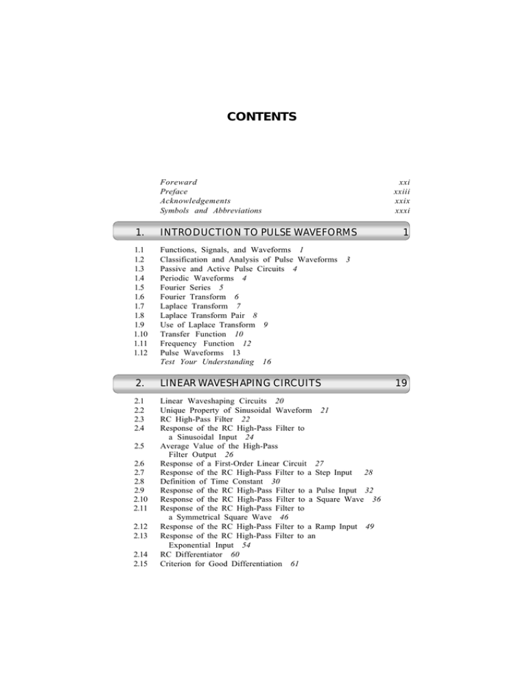
CONTENTS Foreward Preface Acknowledgements Symbols and Abbreviations xxi xxiii xxix xxxi 1. INTRODUCTION TO PULSE WAVEFORMS 1.1 1.2 1.3 1.4 1.5 1.6 1.7 1.8 1.9 1.10 1.11 1.12 Functions, Signals, and Waveforms 1 Classification and Analysis of Pulse Waveforms Passive and Active Pulse Circuits 4 Periodic Waveforms 4 Fourier Series 5 Fourier Transform 6 Laplace Transform 7 Laplace Transform Pair 8 Use of Laplace Transform 9 Transfer Function 10 Frequency Function 12 Pulse Waveforms 13 Test Your Understanding 16 2. LINEAR WAVESHAPING CIRCUITS 2.1 2.2 2.3 2.4 Linear Waveshaping Circuits 20 Unique Property of Sinusoidal Waveform 21 RC High-Pass Filter 22 Response of the RC High-Pass Filter to a Sinusoidal Input 24 Average Value of the High-Pass Filter Output 26 Response of a First-Order Linear Circuit 27 Response of the RC High-Pass Filter to a Step Input 28 Definition of Time Constant 30 Response of the RC High-Pass Filter to a Pulse Input 32 Response of the RC High-Pass Filter to a Square Wave 36 Response of the RC High-Pass Filter to a Symmetrical Square Wave 46 Response of the RC High-Pass Filter to a Ramp Input 49 Response of the RC High-Pass Filter to an Exponential Input 54 RC Differentiator 60 Criterion for Good Differentiation 61 2.5 2.6 2.7 2.8 2.9 2.10 2.11 2.12 2.13 2.14 2.15 1 3 19 xii Contents 2.16 2.17 2.18 2.19 2.20 2.21 2.22 2.23 2.24 2.25 2.26 2.27 2.28 2.29 2.30 3. 3.1 3.2 3.3 3.4 3.5 3.6 3.7 3.8 3.9 3.10 3.11 3.12 3.13 3.14 3.15 3.16 3.17 3.18 3.19 3.20 3.21 3.22 3.23 3.24 3.25 3.26 Op-Amp Differentiator 64 Double Differentiation 66 RC Low-Pass Filter 69 Response of the RC Low-Pass Filter to a Sinusoidal Input 71 Response of the RC Low-Pass Filter to a Step Input 72 Response of the RC Low-Pass Filter to a Pulse Input 74 Response of the RC Low-Pass Filter to a Square Wave 78 Response of the RC low-pass filter to a symmetrical square wave 82 Response of the RC Low-Pass Filter to a Ramp Input 86 Response of the RC Low-Pass Filter to an Exponential Input 93 RC Integrator 95 Criterion for Good Integration 96 RLC Ringing Circuit 99 Uncompensated and Compensated Attenuators 105 Laplace Transform Approach to Uncompensated Attenuator 115 Test Your Understanding 117 NON-LINEAR WAVESHAPING CIRCUITS Non-Linear Waveshaping Circuits 128 Operation of Diode Clipping Circuits 128 Positive Limiting Operation 129 Series-Diode Positive Limiting Circuit 130 Parallel-Diode Positive Limiting Circuit 133 Diode Negative Limiting Operation 139 Series-Diode Clipping Circuit 141 Parallel-Diode Clipping Circuit 143 Practical Considerations 144 Methods for Analyzing Multi-Diode Circuits 145 Method of Assumed States 146 Application of Method of Assumed States 147 Method of Break Point 156 Series-Diode Noise Clipping Circuit 160 Unbiased Noise Clipping Circuit 161 Parallel-Diode Noise Clipping Circuit 162 Double Peak Limiter with Zener Diodes 162 Transistor Clipping Circuit 163 Emitter-Coupled Transistor Clipping Circuit 164 Diode Comparator Circuit 165 Introduction to Clamping Circuits 173 Restoration of the Lost DC Component 174 Clamping a Waveform to Zero Level 175 Simple Diode Circuit that Clamps the Positive Peaks to Zero Self-Adjusting Diode Circuit that Clamps the Positive Peaks to Zero 178 Operation of a Practical Diode Clamping Circuit 181 127 176 Contents 3.27 3.28 3.29 4. 4.1 4.2 4.3 4.4 4.5 4.6 4.7 4.8 4.9 4.10 4.11 4.12 4.13 4.14 4.15 4.16 4.17 4.18 4.19 4.20 4.21 4.22 4.23 4.24 5. 5.1 5.2 5.3 5.4 5.5 5.6 5.7 5.8 5.9 Analysis of a Practical Diode Clamping Circuit 181 Practical Considerations 193 Distortion in the Clamped Waveform at the Reference Voltage Test Your Understanding 199 SWITCHING CHARACTERISTICS OF DEVICES xiii 197 208 Switching Characteristics of a Diode 209 Charge-control Model of a Diode 209 Switching Times in a Diode 210 Breakdown Mechanisms in a Diode 212 Diode Linear Models 213 Switching Times in a Transistor 214 Definitions of Transistor Switching Times 218 Transistor Breakdown Voltages 218 Common-Emitter Transistor Switch 219 Transistor at Saturation 220 Temperature Variation of Saturation Values 221 Transistor at Cut-Off 221 Commutating Capacitance 222 Design of a High-Speed Transistor Switch 224 Schottky Transistor 227 Common-Emitter Switch with Inductive Load 228 Function of Damping Diodes 232 Transistor Switch with Capacitive Load 233 Collector Catching Diodes 237 JFET Switches 240 NMOS and PMOS Switches 241 MOSFET Driver: Passive Load and Active Load 243 CMOS Switch 244 Dynamic Power Dissipation in CMOS Switch 245 Test Your Understanding 247 REGENERATIVE FEEDBACK AND MULTIVIBRATORS Role of Feedback in Electronic Circuits 251 Closed-Loop System 251 Effect of Feedback on Amplifier Parameters 252 Loop Gain 253 Effect of Feedback on Stability 254 Stable, Unstable and Oscillatory Behaviour 255 Sinusoidal Oscillations 256 Principles of Multivibrators 257 Classification of Multivibrators 258 Test Your Understanding 261 250 xiv Contents 6. 6.1 6.2 6.3 6.4 6.5 6.6 6.7 6.8 6.9 6.10 6.11 6.12 6.13 6.14 6.15 7. 7.1 7.2 7.3 7.4 7.5 7.6 7.7 7.8 7.9 7.10 7.11 7.12 7.13 7.14 8. 8.1 8.2 TRANSISTOR BISTABLE MULTIVIBRATORS 265 Classification of Multivibrators 266 Quiescent Condition of a Bistable Multivibrator 269 Fixed-Bias Transistor Bistable Multivibrator 272 Effect of Loading of Collector on Output Swing 272 Collector-Catching Diodes 274 Self-Biased Transistor Bistable Multivibrator 292 Speed-up Capacitors 292 Basic Techniques in the Triggering of Bistable Multivibrators 310 Application of Trigger Input at the Base of the OFF Transistor 312 Application of Trigger Input at the Base of the on Transistor 312 Sensitivity of a Transistor to a Trigger Input 312 Unsymmetrical Triggering of a Bistable Multivibrator 314 Using the Bistable Multivibrator as T Flip-Flop 316 Symmetrical Triggering Applying a Step at the Common Emitters 318 Direct Connected Transistor Bistable Multivibrator 321 Test Your Understanding 323 TRANSISTOR SCHMITT TRIGGER CIRCUIT 327 Schmitt Trigger Circuit 328 Effect of Loop Gain on the Circuit 329 Stable Equilibrium and Unstable Equilibrium 332 Schmitt Trigger Circuit and the Conventional Bistable Multivibrator 332 Hysteresis of the Schmitt Trigger Circuit 334 Applications of the Schmitt Trigger Circuit 335 Aanalysis of a Schmitt Trigger Circuit 336 Comments on the Stability of VUTP in Practice 338 Operating Transistor Q2 in Saturation 339 Need to keep the Hysteresis Gap VH Small 339 Calculation of VLTP of a Schmitt Trigger Circuit 340 Adjustment of VLTP and VUTP for Controlling the Hysteresis Gap 342 Choosing Rs for proper functioning of the Circuit 357 Precautions to be Taken While Using Re1 and Re2 to Control VH 357 Test Your Understanding 358 TRANSISTOR MONOSTABLE AND ASTABLE MULTIVIBRATORS Monostable Multivibrator 364 Triggering of the Collector-Coupled Monostable Multivibrator 363 364 Contents 8.3 8.4 8.5 8.6 8.7 8.8 8.9 8.10 8.11 8.12 8.13 8.14 8.15 8.16 9. 9.1 9.2 9.3 9.4 9.5 9.6 9.7 9.8 9.9 9.10 9.11 9.12 9.13 9.14 9.15 9.16 9.17 9.18 xv Expression for Gate Width T with Q1 in Active Region 367 Expression for Gate Width T with Q1 in Saturation 368 Waveforms of the Collector Coupled Monostable Multivibrator 369 Overshoot @ in Base Waveform of Transistor Q2 at t = T 377 Emitter Coupled Monostable Multivibrator 379 Waveforms of the Emitter-Coupled Monostable Multivibrator 381 Expression for Gate width T 383 Collector-Coupled Transistor Astable Multivibrator 384 Voltage-to-Frequency Converter 390 Astable Multivibrator with Vertical-Edged Collector Waveforms 391 Gated Astable Multivibrator 393 Blocked Condition in an Astable Multivibrator 393 Emitter-Coupled Astable Multivibrator 394 Advantages and Disadvantages of Emitter-Coupled Astable Multivibrator 400 Test Your Understanding 401 VOLTAGE SWEEP CIRCUITS 405 Voltage Sweep Waveform 406 Departure from Linearity of a Voltage Sweep Waveform 407 Relationship between es, et, and ed for an Exponential Waveform 408 Overview of Methods of Generating a Voltage Sweep Waveform 412 Generation of a Voltage Sweep Waveform through Exponential Charging 413 Free-Running Mode Operation 416 Triggered-Mode Operation 416 Free-Running UJT Sweep Waveform Generator 416 Free-Running UJT Circuit with Control-Lable Sweep and Retrace Intervals 419 Triggered UJT Sweep Waveform Generator 423 Transistor Constant-Current Sweep Circuit 428 Basic Principles Common to Miller and Bootstrap Approaches 430 Miller Voltage Sweep Circuit 433 Bootstrap Voltage Sweep Circuit 439 Comparison of Miller Sweep and Bootstrap Sweep Circuits 443 Transistor Miller Voltage Sweep Circuit 444 Single Transistor Bootstrap Voltage Sweep Circuit 446 Two-transistor Bootstrap Voltage Sweep Circuit 448 Test Your Understanding 458 xvi Contents 10. 10.1 10.2 10.3 10.4 10.5 10.6 10.7 10.8 10.9 10.10 11. 11.1 11.2 11.3 11.4 11.5 11.6 11.7 11.8 11.9 11.10 12. 12.1 12.2 12.3 12.4 12.5 12.6 12.7 12.8 12.9 12.10 12.11 CURRENT SWEEP CIRCUITS 463 Principle of Current Sweep Generation 464 Simple Current Sweep 464 Slope Error of the Current Sweep Waveform 466 Linearity Correction through Adjustment of Driving Waveform 468 Complete Practical Current Sweep Generator 472 Omission of Coil Capacitance 474 Circuits for Generating an Impulse 477 Improvement of Linearity of Current Driver for Yoke 478 Linearization of Trapezoidal Voltage 479 Mechanism to Generate a Fast Retrace Current Sweep 480 Test Your Understanding 482 SYNCHRONIZATION AND FREQUENCY DIVISION 485 Two Types of Synchronization 486 Relaxation Circuit 487 Synchronization of a Relaxation Circuit 487 Pulse Synchronization of an Astable Circuit 487 Frequency Division in the Sweep Circuits 489 Synchronization of Astable Multivibrator 490 Monostable Relaxation Circuit as Dividers 493 Phase Delay and Phase Jitters 494 Frequency Division without Phase Jitter 495 Synchronization of a Sweep Circuit with Symmetrical Signals Test Your Understanding 497 SAMPLING GATES Unidirectional Diode Gate 499 General Applications of Sampling Gates 501 Coincidence Gate 501 Unidirectional Diode Sampling Gate Insensitive to – V2 502 Bi-directional Diode Gates 503 Balance Conditions in a Bi-directional Diode Gate 506 Four-Diode Sampling Gate 508 Alternative form of a Four-Diode Sampling Gate 510 Six-Diode Sampling Gate 512 Transistor Sampling Gates 514 Chopper Amplifier 515 Test Your Understanding 517 499 Contents xvii 13. BLOCKING OSCILLATORS 13.1 13.2 13.3 13.4 13.5 13.6 13.7 Pulse Transformers 520 Blocking Oscillators 520 Applications of Blocking Oscillator 520 Triggered Transistor Blocking Oscillator (Base Timing) 521 Triggered Transistor Blocking Oscillator (Emitter Timing) 527 Astable Transistor Blocking Oscillator (Diode-Controlled) 533 Astable Transistor Blocking Oscillator (RC-Controlled) 540 Test Your Understanding 543 14. NETWORK THEOREMS, TRANSIENTS, AND IMPEDANCE MATCHING 14.1 14.2 14.3 14.4 14.5 14.6 14.7 14.8 14.9 14.10 545 Network Theorems 546 Steady-State and Transient Responses 552 Response of a First-Order Linear Circuit 553 Electrical circuit Transients 554 Initial and Final Conditions 555 Properties of Passive Components 555 RC Circuit Transients 558 RL Circuit Transients 559 Voltage and Current Sources 560 Impedance Matching 563 15. REVIEW OF RLC CIRCUITS 15.1 15.2 15.3 15.4 15.5 15.6 Forced Response 567 Natural Response 567 Analysis of an RLC Circuit 567 Response of the RLC Circuit to a Step Waveform 570 Analysis of a Series RLC Circuit 576 Analogy between Electrical Circuits and Mechanical Systems 16. OP-AMP AND IC 555 TIMER 16.1 16.2 16.3 16.4 16.5 16.6 16.7 16.8 16.9 16.10 519 Operational Amplifier 583 Characteristics of an Ideal Op-amp 584 Voltage Constraint and Current Constraint 585 Inverting and Non-Inverting Op-amp Amplifiers 585 Op-amp Non-Inverting Amplifier 587 Simple Op-Amp Applications 588 Op-amp Differentiator 591 Practical Op-amp Differentiator 592 Op-amp Integrator 593 Practical Op-amp Integrator 594 566 581 582 xviii Contents 16.11 16.12 16.13 16.14 16.15 16.16 16.17 16.18 16.19 16.20 16.21 16.22 16.23 17. 17.1 17.2 17.3 17.4 17.5 17.6 17.7 17.8 17.9 17.10 17.11 17.12 17.13 17.14 17.15 18. 18.1 18.2 18.3 18.4 18.5 18.6 18.7 18.8 18.9 18.10 Reasons for Preferring Integrators 594 Op-Amp based Monostable Multivibrator 595 Op-Amp based Astable Multivibrator 598 Inverting Schmitt Trigger Circuit Using Op-Amp 600 IC 555 Timer 603 Monostable Multivibrator with IC 555 Timer 604 Astable Multivibrator with IC 555 Timer 607 Multivibrators Employing Negative-Resistance Devices 609 Operating Point on the Volt–Ampere Characteristic 611 Bistable Operation 616 Monostable Operation 617 Astable Operation 619 Voltage-Controlled NR Switching Circuits 620 Test Your Understanding 621 DIGITAL LOGIC AND FLIP-FLOPS 624 Analog, Digital and Binary Signals 625 Basic Boolean Operations 625 Other Boolean Identities 627 NAND and NOR as the Universal Gates 627 NAND Realization 628 NOR Realization 629 Design of a Combinational Logic Circuit 629 Design of a Full Adder 630 Sequential Logic Circuits 632 SR Latch 633 Clocked SR Flip-Flop 634 JK Flip-Flop 636 Level-Triggered and Edge Triggered Flip-Flops 637 Master-Slave JK Flip-Flop 637 Registers and Counters 638 REVIEW OF SEMICONDUCTOR DIODES AND TRANSISTORS Composition of Matter 642 Classification of Matter 642 Improving Conductivity of Semiconductors 644 Generation and Recombination of Hole-Electron Pairs Controlled-Flow of Charge Carriers 645 Majority and Minority Carriers 646 Drift and Diffusion Currents 646 Semiconductor Diode Operation 647 Diode Characteristic 649 Concept of Load Line 652 644 641 Contents 18.11 18.12 18.13 xix Bipolar Junction Transistor 652 Transistor Biasing Circuits 655 Unijunction Transistor (UJT) 658 Appendix Index 661 664


