CCD-based Range-finding Sensor
advertisement

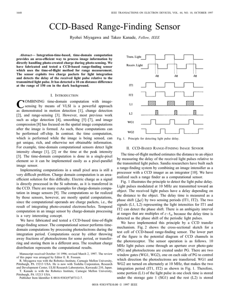
1648 IEEE TRANSACTIONS ON ELECTRON DEVICES, VOL. 44, NO. 10, OCTOBER 1997 CCD-Based Range-Finding Sensor Ryohei Miyagawa and Takeo Kanade, Fellow, IEEE Abstract— Integration-time-based, time-domain computation provides an area-efficient way to process image information by directly handling photo-created charge during photo-sensing. We have fabricated and tested a CCD-based range-finding sensor which uses the time-of-flight method for range measurement. The sensor exploits two charge packets for light integration and detects the delay of the received light pulse relative to the transmitted light pulse. It has detected a 10 cm distance difference at the range of 150 cm in the dark background. I. INTRODUCTION C OMBINING time-domain computation with imagesensing by means of VLSI is a powerful approach as demonstrated in motion detection [1], change detection [2], and range-sensing [3]. However, most previous work such as edge detection [4], smoothing [5]–[7], and image compression [8] has focused on the spatial image computations after the image is formed. As such, these computations can be performed off-chip. In contrast. the time computation, which is performed while the image is being sensed, can get unique, rich, and otherwise not obtainable information. For example, time-domain computational sensors detect light intensity change [1], [2] or the time at the peak intensity [3]. The time-domain computation is done in a single-pixel element so it can be implemented easily as a pixel-parallel image sensor. Implementing computations in a small pixel area is still a very difficult problem. Charge domain computation is an areaefficient solution for this difficulty. Electric charge as a signal is directly processed in the Si substrate, as it is transferred in the CCD. There are many examples for charge-domain computation in image sensors [9]. The computations so far realized by those sensors, however, are mostly spatial computations, since the computational operands are charge packets, i.e., the result of integrating photo-created electrons/holes. Temporal computation in an image sensor by charge-domain processing is a very interesting concept. We have fabricated and tested a CCD-based time-of-flight range-finding sensor. The computational sensor performs timedomain computations by processing photoelectrons during the integration period. Computations occur by either throwing away fractions of photoelectrons for some period, or transferring and storing them in a different area. The resultant charge distribution represents the computational results. Manuscript received October 14 1996; revised March 2, 1997. The review of this paper was arranged by Editor E. R. Fossum. R. Miyagawa was with the Robotics Institute, Carnegie Mellon University, Pittsburgh, PA 15213 USA. He is now with Toshiba Corporation, Research and Development Center, ULSI Research Laboratories, Kawasaki 210, Japan. T. Kanade is with the Robotics Institute, Carnegie Mellon University, Pittsburgh, PA 15213 USA. Publisher Item Identifier S 0018-9383(97)07312-7. Fig. 1. Principle for detecting light pulse delay. II. CCD-BASED RANGE-FINDING IMAGE SENSOR The time-of-flight method estimates the distance to an object by measuring the delay of the received light pulses relative to the transmitted light pulses. Sandia researchers have built such a range-finding system by combining an image intensifier as a processor with a CCD imager as an integrator [10]. We have realized such a range finder as a computational sensor. Fig. 1 illustrates the principle to detect the light pulse delay. Light pulses modulated at 10 MHz are transmitted toward an object. The received light pulses have a delay depending on the distance to the object. The delay time is measured as a phase shift by two sensing periods (IT1, IT2). The two signals (L1, L2) representing the light intensities for IT1 and IT2 can detect the phase shift. There is an ambiguity interval at ranges that are multiples of because the delay time is detected as the phase shift of the periodic light pulses. We have implemented this principle by a CCD transfer mechanism. Fig. 2 shows the cross-sectional sketch for a test cell of CCD-based range-finding sensor. The lower part of the figure is the potential diagram of CCD channels in the photoreceptor. The sensor operation is as follows. 10 MHz light pulses come through an aperture over photo-gate (PG) and photoelectrons are created under PG. There are two window gates (WG1, WG2), one on each side of PG to control which direction the photoelectrons are transferred. WG1 and WG2 are turned on alternately at 10 MHz, that makes the two integration period (IT1, IT2) as shown in Fig. 1. Therefore, some portion (L1) of the light pulse in one clock time is stored under the storage gate 1 (SG1) and the rest (L2) is stored 0018–9383/97$10.00 1997 IEEE MIYAGAWA AND KANADE: CCD-BASED RANGE-FINDING SENSOR 1649 storage gates. This direct leakage effect needs to be taken into account when calculating the range. W1:Off W2:Off Output1 mV mV Output2 mV mV The range estimation can be done as follows. Let and be photo-charges transferred by the window gate 1 and 2, respectively. Let and the photo-charges leaked into the storage gate 1 and 2, respectively. Therefore, the and observed Output1 and Output2 are the sums of , respectively. The light-pulse-phase shift determines the relative distance. Therefore, the relative range can be estimated by Fig. 2. Cross-sectional sketch and potential diagram for CCD-based range-finder pixel. under the storage gate 2 (SG2). The portion is determined by the temporal position of the light pulse relative to the window gate pulses. Conversely, the storage charge difference between SG1 and SG2 gives the light delay relative to the window gate timing. The operation of distributing charge to the two packets repeats with a series of light pulses for a certain period to integrate enough signal charge under the storage gates. The integrated charges are transferred through OG to the detection nodes (FD1, FD2) which are connected to output amplifiers. where is the light velocity and , the pulse width. All the charges are linear to the total charge It can be assumed that We can simplify this expression by noting represents the real, temporal light-pulse position. The estimated range is expressed as follows: III. TEST CELL EXPERIMENT We have fabricated a test cell and verified its operation. The chip was illuminated directly by a light pulse, which was created by a LED, and whose delay time was controlled by a programmable delay line. The wavelength of the LED was 592 nm and its response time was 13 ns, fast enough for the 10 MHz drive. The least step for the delay line was 0.25 ns. The measurement results were plotted against the delay time in Fig. 3. Output1 first increased with the delay time and then decreased. Output2 was the exact opposite of Output1. The sum of Output1 and Output2 was almost the same. Output1 and Output2 can be regarded as in-phase and out-of-phase components, respectively. The light pulse becomes in-phase with increasing delay and was fully in-phase at the peak of Output1. It went out-of-phase after the peak. This result has shown that the photoelectrons were successfully differentiated according to the window periods. Note that the Output2 value at the bottom was much larger than zero, though the light pulse was fully in-phase. In order to investigate this phenomena, we measured both outputs by turning off one window gate pulse at 0 ns delay time. The result was listed in the table below. Both outputs have significant voltage output without the window gate pulses. These value were very close. This means that the photoelectrons created in deep depth directly entered each storage area, regardless of the window gate operation. The cause of this small difference could be a small shift of the aperture from the center of two for for where and is an integer or zero. The value of was 0.86 with the data listed in the previous table. The effect of the leakage charge is easy to compensate for by the calibration of this scale factor. The offset is the phase difference between the light pulses and the timing pulses, which is caused by the driving circuit for the sensor and the light source. To calibrate this offset, an object at a certain distance was observed by the range-finding sensor. Then, the offset is determined so that the resultant range coincides with the resultant one. The represents an ambiguity interval at ranges caused by the periodicity of the phase shift between light pulses and the window gate timing pulses. When measuring range beyond , the sensor has this ambiguity. A technique using multiple-frequency pulses for this problem was reported [10]. Please see the reference for the details. The for 10 MHz drive is 15 m. In the experiment in Section IV, the measured range was less than this 15 m. Therefore, the experiment did not suffer from this ambiguity. The dark current is constant independent of the light intensity. The dark current is simply an offset. So, if the dark current is measured first, it can subtracted from the photo-charges. 1650 IEEE TRANSACTIONS ON ELECTRON DEVICES, VOL. 44, NO. 10, OCTOBER 1997 Fig. 3. Test cell outputs versus delay time. Fig. 5. Chip photograph of range-finding linear sensor. Fig. 4. Range-finding linear sensor structure. IV. ONE-DIMENSIONAL-ARRAY RANGE-FINDING SENSOR Fig. 4 shows the structure for a range-finding onedimensional-array sensor. The linear sensor has a similar cell structure to the test photo-cell. The difference is that the line sensor transfers both signal charges in the same direction to a detection node after signal charge integration. All the gates function as a 4-phase drive CCD when transferring the signal charges. The electrons are held in the channel of high potential. The channel potential controlled by the gate voltage. In the CCD charge transfer, the signal charge is held under the gate at a high level. Therefore, the charge is transferred by changing the voltages of the gates serially. When using a 4-drive pulse of different phase, the transfer channel is called 4-phase drive CCD. The signal charges which reach their detection nodes are read-out by source-followers. Each detection node is serially scanned by a shift-register. A 32pixel line sensor was fabricated by MOSIS with the Orbit 2- m Analog process. The size of each pixel is m Fig. 5 is the chip photograph of the linear sensor. Fig. 6 shows the sketch of the driving pulses for the sensor. The period between and is the light integration time. The driving pulses, illustrated in Fig. 1, are applied to the window gates in this period. The two signal charges are integrated under the storage gates. WG1 and TG2 go high at the time Then, one signal charge is stored under WG1 and SG1, the other is stored under TG2 and SG2. The signal charges are transferred toward the detection node by applying the 4phase drive pulses to all the gates other than BG, OG and RS and The first signal charge reaches under BG between while the second signal charge is under SG2 at the time and TG2. Then, the RS goes low and the reset levels of the detection nodes are read out by using the shift register between and The BG goes low and the signal charge is transferred to the detection node through the OG. Then, the signal levels The first at the detection nodes are read out between and MIYAGAWA AND KANADE: CCD-BASED RANGE-FINDING SENSOR 1651 Fig. 6. Drive pulses for range finder. Fig. 8. Range measurement setup. Fig. 7. Sensor output oscilloscope waveform. signal charges are read out in this way. The second ones are and read out by continuing the pulse scheme between Fig. 7 shows the waveform of the sensor output observed by an oscilloscope. The waveform has four regions corresponding to the reset levels, the signal levels for the first signal charges and those for the second signal charges. Fig. 8 shows the setup for the range measurement. We mounted camera optics on the line sensor. The LED array as a light source was placed neighboring to the camera. The sensor output was buffered and digitized by an AD converter. The digitized data was taken by a workstation where the range was calculated. A white plate was placed in front of the camera at various distances. The range was estimated by using the equation described in the Section III. We found the sensor sensitivity to be very low because of the thick 6000 Å polysilicon PG, the signal charges were integrated for 1.06 s. There was also significant dark current with the long integration period, which caused much noise. The experiment was done in dark background. The estimated distance is plotted in Fig. 9. In principle, the time-of-flight measurement Fig. 9. Range estimation. detects the phase difference, so that the estimated distance needs to be calibrated. The distance data in Fig. 9 wasn’t calibrated. Therefore, the estimated range in Fig. 9 has offset. The horizontal axis is the distance of the plate from the camera. The estimated distance increases linearly with the real distance. The slope of the curve was 0.9 and it roughly coincided to the of 0.86 given by the test cell experiment. We also tried to measure the structured object. The plate that has a rectangle hole in the center was placed at the distance of 150 cm from the camera. Another plate was also placed behind the plate at various distances from it. The distances between the two plates were 5, 10, and 15 cm. The range-finder camera observed the plate behind and through the hole of the front plate. The range 1652 IEEE TRANSACTIONS ON ELECTRON DEVICES, VOL. 44, NO. 10, OCTOBER 1997 not obtainable by the spatial processing. This sensor’s unique capability has shown that the time-domain computation at the level of phototransduction is a powerful methodology. REFERENCES [1] T. Delbruck, “Silicon retina with correlation-based, velocity-tuned pixels,” IEEE Trans. Neural Network, vol. 4, pp. 529–541, 1993. [2] T. Delbruck and C. A. Mead, “Time-derivative adaptive silicon photoreceptor array,” in Proc. SPIE, vol. 1541, 1993, pp. 92–99. [3] A. Gruss et al., “Integrated sensor and range-finding analog signal processor,” IEEE J. Solid-State Circuit, vol. 26, pp. 184–190, 1991. [4] J. G. Harris et al., “Two-dimensional analog VLSI circuit for detecting discontinuities,” Science, vol. 248, pp. 1209–1211, 1990. [5] P. C. Yu et al., “CMOS resistive fuses for image smoothing and segmentation,” IEEE J. Solid-State Circuits, vol. 27, pp. 545–552, 1992. [6] H. Kobayashi et al., “An analog CMOS network for gaussian convolution with embedded image sensing,” in Tech. Dig. ISSCC 1990, pp. 216–217. [7] C. L. Keast et al., “A CCD/CMOS-based imager with integrated focal plane signal processing,” IEEE J. Solid-State Circuits, vol. 28, pp. 431–437, 1993. [8] S. E. Kemeny et al., “CCD focal-plane image reorganization processors for lossless image compression,” IEEE J. Solid-State Circuits, vol. 27, pp. 398–405, 1992. [9] W. Yang and A. Chiang, “A full fill-factor CCD imager with integrated signal processors,” in Tech. Dig. ISSCC 1990, pp. 218–219. [10] J. P. Anthes et al., “Non-scanned RADAR imaging and application,” in Proc. SPIE, vol. 1936, 1993, pp. 11–21. Fig. 10. Range estimation for structured object. was also measured with the plate without a hole placed at the distance of 150 cm. The data was used to calibrate the range data for the structured object. The calibrated range results were plotted in Fig. 10. The base lines of the three range results coincided to the 150 cm. The 10 cm distance was found to be detected though the 5 cm distance was within the noise level. V. CONCLUSION The CCD-based range finder using the time-of-flight method has been fabricated and tested. The sensor could detect the distance difference of 10 cm at the range of 150 cm in the dark background. The sensor measured the phase shift between the transmitted light pulse and the received light pulse for the range measurement. The sensor exploited two photo-created charge packets whose integration time were modulated with the light-pulse frequency. Photoelectrons were separated into those two charge packets by transferring through two window gates. The integration time for the two charge packets was modulated by the drive pulse timing for the two window gates. The charge level, time-domain processing was areaefficient and provided the unique information, range, which is Ryohei Miyagawa was born in Tokyo, Japan, in 1958. He received the B.S. degree in physics and the M.S. degree in electrical engineering from Tokyo Institute of Technology, in 1982 and 1984, respectively. He joined Toshiba Corporation in 1984 and now works at the ULSI Research Laboratories, R&D Center, Kawasaki, Japan. Since he joined Toshiba, he has been engaged in researching and developing two-level image sensors. He stayed at the Robotics Institute, Carnegie Mellon University, Pittsburgh, PA, as a Visiting Scientist from 1993 to 1995. Mr. Miyagawa is a member of the Japan Society of Applied Physics and the Institute of Television Engineers of Japan. Takeo Kanade (M’80–SM’88–F’92) received the Doctoral degree in electrical engineering from Kyoto University, Kyoto, Japan, in 1974. After holding a faculty position at the Department of Information Science, Kyoto University, he joined Carnegie Mellon University, Pittsburgh, PA, in 1980, where he is currently U. A. Helen Whitaker Professor of Computer Science and Director of the Robotics Institute. He has written more than 150 technical papers on computer vision, sensors, and robotics systems. Dr. Kanade is a Founding Fellow of American Association of Artificial Intelligence. He was a recipient of the Joseph Engelberger Award in 1995. He has served on many government, industry, and university advisory or consultant committees, including Aeronautics and Space Engineering Board (ASEB) of National Research Council, NASA’s Advanced Technology Advisory Committee (Congressionally Mandate Committee), and Advisory Board of Canadian Institute for Advanced Research.


