breadboard implementation of a reduced instruction set processor
advertisement

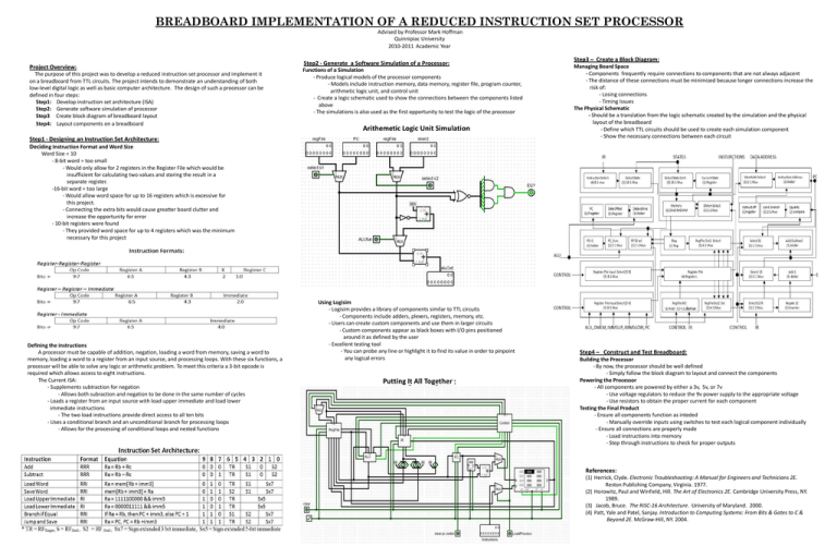
BREADBOARD IMPLEMENTATION OF A REDUCED INSTRUCTION SET PROCESSOR Advised by Professor Mark Hoffman Quinnipiac University 2010-2011 Academic Year Project Overview: The purpose of this project was to develop a reduced instruction set processor and implement it on a breadboard from TTL circuits. The project intends to demonstrate an understanding of both low-level digital logic as well as basic computer architecture. The design of such a processor can be defined in four steps: Step1: Develop instruction set architecture (ISA) Step2: Generate software simulation of processor Step3 Create block diagram of breadboard layout Step4: Layout components on a breadboard Step2 - Generate a Software Simulation of a Processor: Functions of a Simulation - Produce logical models of the processor components - Models include instruction memory, data memory, register file, program counter, arithmetic logic unit, and control unit - Create a logic schematic used to show the connections between the components listed above - The simulations is also used as the first opportunity to test the logic of the processor Arithemetic Logic Unit Simulation Step1 - Designing an Instruction Set Architecture: Deciding Instruction Format and Word Size Step3 – Create a Block Diagram: Managing Board Space - Components frequently require connections to components that are not always adjacent - The distance of these connections must be minimized because longer connections increase the risk of: - Losing connections - Timing Issues The Physical Schematic - Should be a translation from the logic schematic created by the simulation and the physical layout of the breadboard - Define which TTL circuits should be used to create each simulation component - Show the necessary connections between each circuit Word Size = 10 - 8-bit word = too small - Would only allow for 2 registers in the Register File which would be insufficient for calculating two values and storing the result in a separate register. -16-bit word = too large - Would allow word space for up to 16 registers which is excessive for this project. - Connecting the extra bits would cause greatter board clutter and increase the opportunity for error - 10-bit registers were found - They provided word space for up to 4 registers which was the minimum necessary for this project Defining the instructions A processor must be capable of addition, negation, loading a word from memory, saving a word to memory, loading a word to a register from an input source, and processing loops. With these six functions, a processor will be able to solve any logic or arithmetic problem. To meet this criteria a 3-bit opcode is required which allows access to eight instructions. The Current ISA: - Supplements subtraction for negation - Allows both subraction and negation to be done in the same number of cycles - Loads a register from an input source with load upper immediate and load lower immediate instructions - The two load instructions provide direct access to all ten bits - Uses a conditional branch and an unconditional branch for processing loops - Allows for the processing of conditional loops and nested functions Using Logisim - Logisim provides a library of components similar to TTL circuits - Components include adders, plexers, registers, memory, etc. - Users can create custom components and use them in larger circuits - Custom components appear as black boxes with I/O pins positioned around it as defined by the user - Excellent testing tool - You can probe any line or highlight it to find its value in order to pinpoint any logical errors Putting It All Together Step4 – Construct and Test Breadboard: Building the Processor - By now, the processor should be well defined - Simply follow the block diagram to layout and connect the components Powering the Processor - All components are powered by either a 3v, 5v, or 7v - Use voltage regulators to reduce the 9v power supply to the appropriate voltage - Use resistors to obtain the proper current for each component Testing the Final Product - Ensure all components function as inteded - Manually override inputs using switches to test each logical component individually - Ensure all connections are properly made - Load instructions into memory - Step through instructions to check for proper outputs References: (1) Herrick, Clyde. Electronic Troubleshooting: A Manual for Engineers and Technicians 2E. Reston Publishing Company, Virginia. 1977. (2) Horowitz, Paul and Winfield, Hill. The Art of Electronics 2E. Cambridge University Press, NY. 1989. (3) Jacob, Bruce. The RiSC-16 Architecture. University of Maryland. 2000. (4) Patt, Yale and Patel, Sanjay. Introduction to Computing Systems: From Bits & Gates to C & Beyond 2E. McGraw-Hill, NY. 2004.

