Submillisecond response nematic liquid crystal modulators using
advertisement

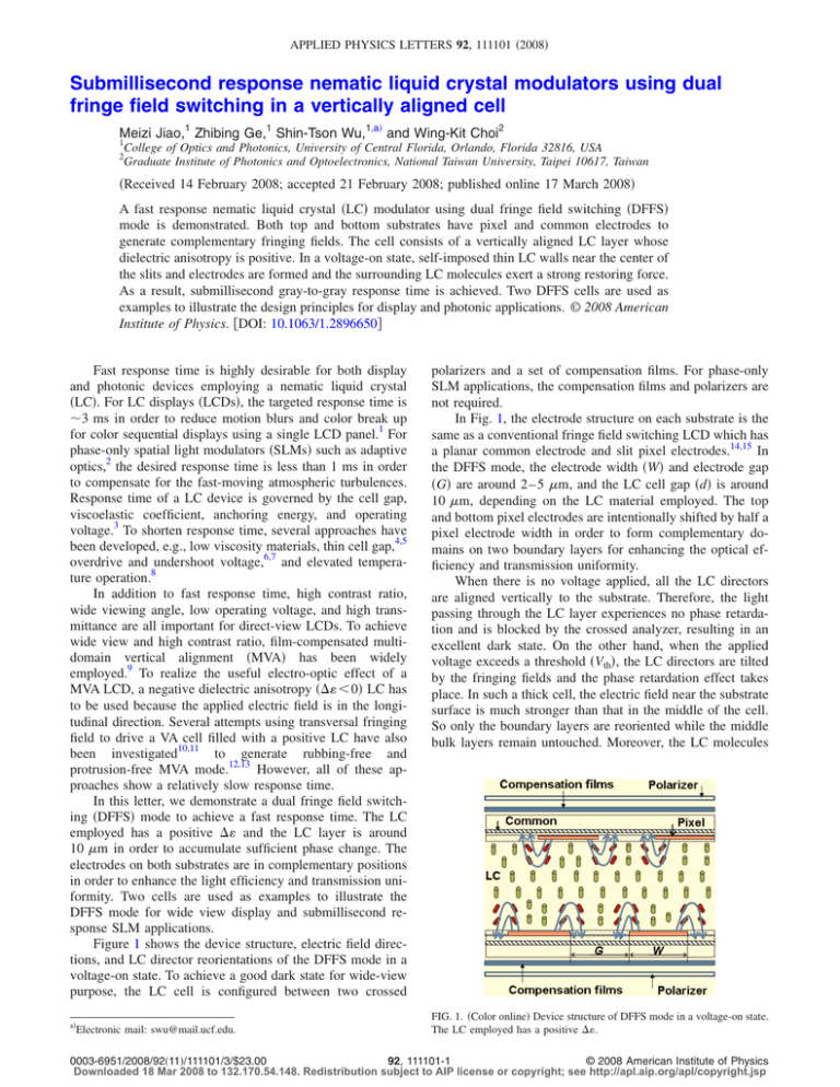
APPLIED PHYSICS LETTERS 92, 111101 共2008兲 Submillisecond response nematic liquid crystal modulators using dual fringe field switching in a vertically aligned cell Meizi Jiao,1 Zhibing Ge,1 Shin-Tson Wu,1,a兲 and Wing-Kit Choi2 1 College of Optics and Photonics, University of Central Florida, Orlando, Florida 32816, USA Graduate Institute of Photonics and Optoelectronics, National Taiwan University, Taipei 10617, Taiwan 2 共Received 14 February 2008; accepted 21 February 2008; published online 17 March 2008兲 A fast response nematic liquid crystal 共LC兲 modulator using dual fringe field switching 共DFFS兲 mode is demonstrated. Both top and bottom substrates have pixel and common electrodes to generate complementary fringing fields. The cell consists of a vertically aligned LC layer whose dielectric anisotropy is positive. In a voltage-on state, self-imposed thin LC walls near the center of the slits and electrodes are formed and the surrounding LC molecules exert a strong restoring force. As a result, submillisecond gray-to-gray response time is achieved. Two DFFS cells are used as examples to illustrate the design principles for display and photonic applications. © 2008 American Institute of Physics. 关DOI: 10.1063/1.2896650兴 Fast response time is highly desirable for both display and photonic devices employing a nematic liquid crystal 共LC兲. For LC displays 共LCDs兲, the targeted response time is ⬃3 ms in order to reduce motion blurs and color break up for color sequential displays using a single LCD panel.1 For phase-only spatial light modulators 共SLMs兲 such as adaptive optics,2 the desired response time is less than 1 ms in order to compensate for the fast-moving atmospheric turbulences. Response time of a LC device is governed by the cell gap, viscoelastic coefficient, anchoring energy, and operating voltage.3 To shorten response time, several approaches have been developed, e.g., low viscosity materials, thin cell gap,4,5 overdrive and undershoot voltage,6,7 and elevated temperature operation.8 In addition to fast response time, high contrast ratio, wide viewing angle, low operating voltage, and high transmittance are all important for direct-view LCDs. To achieve wide view and high contrast ratio, film-compensated multidomain vertical alignment 共MVA兲 has been widely employed.9 To realize the useful electro-optic effect of a MVA LCD, a negative dielectric anisotropy 共⌬ ⬍ 0兲 LC has to be used because the applied electric field is in the longitudinal direction. Several attempts using transversal fringing field to drive a VA cell filled with a positive LC have also been investigated10,11 to generate rubbing-free and protrusion-free MVA mode.12,13 However, all of these approaches show a relatively slow response time. In this letter, we demonstrate a dual fringe field switching 共DFFS兲 mode to achieve a fast response time. The LC employed has a positive ⌬ and the LC layer is around 10 m in order to accumulate sufficient phase change. The electrodes on both substrates are in complementary positions in order to enhance the light efficiency and transmission uniformity. Two cells are used as examples to illustrate the DFFS mode for wide view display and submillisecond response SLM applications. Figure 1 shows the device structure, electric field directions, and LC director reorientations of the DFFS mode in a voltage-on state. To achieve a good dark state for wide-view purpose, the LC cell is configured between two crossed a兲 Electronic mail: swu@mail.ucf.edu. polarizers and a set of compensation films. For phase-only SLM applications, the compensation films and polarizers are not required. In Fig. 1, the electrode structure on each substrate is the same as a conventional fringe field switching LCD which has a planar common electrode and slit pixel electrodes.14,15 In the DFFS mode, the electrode width 共W兲 and electrode gap 共G兲 are around 2 – 5 m, and the LC cell gap 共d兲 is around 10 m, depending on the LC material employed. The top and bottom pixel electrodes are intentionally shifted by half a pixel electrode width in order to form complementary domains on two boundary layers for enhancing the optical efficiency and transmission uniformity. When there is no voltage applied, all the LC directors are aligned vertically to the substrate. Therefore, the light passing through the LC layer experiences no phase retardation and is blocked by the crossed analyzer, resulting in an excellent dark state. On the other hand, when the applied voltage exceeds a threshold 共Vth兲, the LC directors are tilted by the fringing fields and the phase retardation effect takes place. In such a thick cell, the electric field near the substrate surface is much stronger than that in the middle of the cell. So only the boundary layers are reoriented while the middle bulk layers remain untouched. Moreover, the LC molecules FIG. 1. 共Color online兲 Device structure of DFFS mode in a voltage-on state. The LC employed has a positive ⌬. 0003-6951/2008/92共11兲/111101/3/$23.00 92, 111101-1 © 2008 American Institute of Physics Downloaded 18 Mar 2008 to 132.170.54.148. Redistribution subject to AIP license or copyright; see http://apl.aip.org/apl/copyright.jsp 111101-2 Appl. Phys. Lett. 92, 111101 共2008兲 Jiao et al. The voltage-dependent transmittance 共VT兲 of cell 1 is shown as curve 1 in Fig. 2, whose threshold voltage is Vth ⬃ 2.5 Vrms, on-state voltage Von ⬃ 13 Vrms, and maximum transmittance Tmax ⬃ 91.8% 共normalized to the maximum transmittance of two parallel linear polarizers兲. Meanwhile, we use cell 2 as an example for photonic applications. The cell gap is d = 11 m, W = 2 m, and G = 2 m. With decreased electrode width and gap, the tilted LC layer shrinks closer to the substrate, which means that fewer LC molecules contribute to the phase retardation effect. Therefore, a higher birefringence LC material is required to obtain a sufficient phase change. Curve 3 in Fig. 2 represents the VT curve for cell 2 using the E7-like material. Clearly, its phase retardation is insufficient to reach 1 at 15 Vrms. Increasing cell gap does not lower the operating voltage much because it only thickens the unswitched middle layer which makes no contribution to the overall phase retardation. A more effective way is to employ a high ⌬n LC mixture. The parameters for the high birefringence LC material 共UCF-2 type兲18,19 used in calculation are listed as follows: K11 = 17.3 pN, K22 = 10.4 pN, K33 = 38.3 pN, ⌬n = 0.416, ⌬ = 18.27, and ␥1 = 200 mPa s. The VT curve for cell 2 filled with UCF-2 is shown as curve 2 in Fig. 2, where Vth ⬃ 3 Vrms and Tmax ⬃ 93% at Von ⬃ 13 Vrms. The gray-to-gray 共GTG兲 response times of cell 1 and cell 2 were calculated and results are summarized in Tables I and II, respectively. During calculations, we divided the VT curve uniformly into eight gray levels 共1–8兲. Each of the GTG response time was calculated. Here, the response time is defined as 10%–90% transmittance change. The cell gaps of the proposed two cells are optimized to achieve a fast response time. If the cells are too thin, the middle LC layers will rotate slightly with a slower speed which, in turn, leads to a slower GTG response time. On the other hand, if the gap is too thick, some problems such as narrow viewing angle and strong cross-talks between the neighboring pixels would occur. The optimized cell gaps, which depend on the LC material employed, are 14 and 11 m for cell 1 and cell 2, respectively. The average GTG rise time for cell 1 is 1.88 ms and average GTG decay time is 1.68 ms, which are fast enough for color sequential displays. To further shorten response time, a lower viscosity LC or overdrive and undershoot voltage method can be employed. By combining these two effects, the response time is expected to be reduced by additional approximately three to five times. For cell 2, the average GTG rise time is 0.91 ms and decay time is 0.68 ms at room temperature. In comparison, a VA cell with d = 4.64 m 共MLC-6608兲 has an average GTG rise time of FIG. 2. 共Color online兲 Simulated VT curves for proposed cells. Curve 1 is for cell 1 with E7-like LC: d = 14 m, W = 3 m, and G = 3 m; Curve 2 is for cell 2 with high ⌬n LC material: d = 11 m, W = 2 m, and G = 2 m; Curve 3, a comparison curve, is for a cell with E7-like LC: d = 14 m, W = 3 m, and G = 3 m. at the center of each electrode and electrode gap are not tilted because in these regions, the electric fields are too weak to reorient the LC directors. These unswitched LC directors form disclination lines which function as boundary walls to impose a strong restoring force, as shown in Fig. 1. Therefore, fast rise and decay times can be achieved. From Fig. 1, the LC directors form two domains near each substrate surface because of the strong fringe fields. If we use the zigzag electrodes, a four-domain structure will be formed which in turn contributes to wide viewing angle after film compensation. Moreover, the LC reorientation shown in Fig. 1 is similar to the bend structure of a pi cell16 in the lateral direction. This would minimize the backflow effect and lead to a fast response time. The structures and performances of the proposed DFFS mode are optimized using a commercial three-dimensional LC simulator 共TECHWIZ developed by Sanayi兲 and the optical calculation is based on the extended 2 ⫻ 2 Jones matrix methods.17 To obtain fast response time, high transmittance, and wide viewing angle for display applications, we use cell 1 as an example. The device parameters for cell 1 are listed as follows: cell gap d = 14 m, electrode width W = 3 m, and electrode gap G = 3 m. The LC material used in simulations is basically the same as Merck E7 except for a lower viscosity: K11 = 11.7 pN, K22 = 8.8 pN, K33 = 19.5 pN, ⌬n = 0.223, ⌬ = 14.4, and ␥1 = 150 mPa s. For comparison, the rotational viscosity of E7 is ␥1 ⬃ 250 mPa s at room temperature 共⬃22 ° C兲. Some LC mixtures with similar birefringence but with a lower viscosity 共␥1 ⬃ 80 mPa s兲 are commercially available. A lower viscosity leads to a faster response time. TABLE I. Calculated GTG scale response time 共in unit of ms兲 of cell 1. 1 1 2 3 4 5 6 7 8 1.05 1.05 1.09 1.13 1.34 1.25 1.46 2 3 4 5 6 7 8 5.42 3.40 2.62 2.86 2.30 2.24 2.53 1.85 2.10 2.36 1.96 1.58 1.97 2.00 2.48 1.68 1.42 1.58 1.72 1.79 2.44 0.95 0.80 0.77 0.92 0.91 0.95 1.25 1.96 2.12 1.93 1.93 1.96 2.17 2.20 2.03 2.02 2.11 2.36 2.53 2.03 2.21 2.74 3.26 2.56 3.12 3.00 3.44 4.13 Downloaded 18 Mar 2008 to 132.170.54.148. Redistribution subject to AIP license or copyright; see http://apl.aip.org/apl/copyright.jsp 111101-3 Appl. Phys. Lett. 92, 111101 共2008兲 Jiao et al. TABLE II. Calculated GTG scale response time 共in unit of ms兲 of cell 2. 1 1 2 3 4 5 6 7 8 0.37 0.37 0.38 0.40 0.42 0.45 0.53 2 3 4 5 6 7 8 1.70 1.33 1.05 1.24 1.04 1.11 1.20 1.02 0.98 1.22 1.13 0.95 0.90 0.91 1.22 1.00 0.83 0.90 0.75 0.80 1.06 0.60 0.48 0.43 0.40 0.39 0.44 0.53 0.72 0.70 0.69 0.68 0.70 0.80 0.69 0.70 0.71 0.77 0.86 0.68 0.70 0.74 0.90 ⬃38.8 ms and decay time of ⬃42.1 ms.20 The response time of our DFFS mode is ⬃20 times faster. Cell 1 is used as an example for display applications. To obtain a wide viewing angle, we use an A+ plate and a C− plate on each side of the cell. This configuration is quite common for wide view display devices.9 The optic axis of the A+ plate is parallel to the transmission axis of the polarizer on the same side. The parameters of the compensation films used in our simulation are listed as follows: For A+ plate, ne = 1.5590, no = 1.5866, and d = 25.65 m; for C− plate, ne = 1.50, no = 1.65, and d = 8.02 m.21 Figure 3 shows the isocontrast contour plots of film-compensated cell 1. The 100:1 isocontrast contour line extends beyond the 70° viewing cone. This is adequate for most display applications, including televisions, monitors, and mobile devices. However, it is quite difficult to achieve a good dark state for cell 2 because its d⌬n is too large to be compensated precisely. With the employed large d⌬n, the accumulated phase retardation is quite large even under a very small pretilt angle resulting in a non-negligible light leakage. Thus, cell 2 is 0.66 0.72 0.92 0.68 1.04 0.96 more suitable for laser beam steering and adaptive optics where the incident laser beam is nearly normal to the LC cell. The incident laser polarization should be set parallel to the LC reorientation axis 共horizontal direction in Fig. 1兲 in order to obtain phase-only modulation. For such applications, the required phase change is 2. This can be achieved by using reflective mode, where the incident light traverses the LC layer twice, or by increasing the LC birefringence. In conclusion, a submillisecond GTG response DFFS LC mode is demonstrated. This mode has potential applications for displays and phase-only applications. For display applications, the operating voltage needs to be decreased in order to lower power consumption. To lower the on-state voltage, we need to optimize the electrode structures, cell gap, and LC parameters. For phase-only modulations, we need to increase the phase change to 2. This can be done by using a reflective device, increasing the LC birefringence, or further optimizing the device configuration. J. H. Lee, X. Zhu, and S. T. Wu, J. Disp. Technol. 3, 2 共2007兲. D. Gu, B. Winker, B. Wen, D. Taber, A. Brackley, A. Wirth, M. Albanese, and F. Landers, Proc. SPIE 5553, 68 共2004兲. 3 S. T. Wu and D. K. Yang, Reflective Liquid Crystal Displays 共Wiley, New York, 2001兲. 4 S. Gauza, X. Zhu, S. T. Wu, W. Piecek, and R. Dabrowski, J. Disp. Technol. 3, 250 共2007兲. 5 M. Jiao, Z. Ge, Q. Song, and S. T. Wu, Appl. Phys. Lett. 92, 061102 共2008兲. 6 S. T. Wu and C. S. Wu, J. Appl. Phys. 65, 527 共1989兲. 7 S. T. Wu, Appl. Phys. Lett. 57, 986 共1990兲. 8 S. T. Wu, A. M. Lackner, and U. Efron, Appl. Opt. 26, 3441 共1987兲. 9 Q. Hong, T. X. Wu, X. Zhu, R. Lu, and S. T. Wu, Appl. Phys. Lett. 86, 121107 共2005兲. 10 R. A. Soref, J. Appl. Phys. 45, 5466 共1974兲. 11 W. K. Choi and S. T. Wu, U.S. Patent No. 7,298,445 B1 共20 November 2007兲. 12 S. H. Lee, H. Y. Kim, I. C. Park, B. G. Rho, J. S. Park, H. S. Park, and C. H. Lee, Appl. Phys. Lett. 71, 2851 共1997兲. 13 S. H. Hong, Y. H. Jeong, H. Y. Kim, H. M. Cho, W. G. Lee, and S. H. Lee, J. Appl. Phys. 87, 8259 共2000兲. 14 C. Z. Xiang, X. W. Sun, and X. Y. Jin Appl. Phys. Lett. 83, 5154 共2003兲. 15 H. Y. Kim, G. R. Jeon, D. S. Seo, M. H. Lee, and S. H. Lee, Jpn. J. Appl. Phys., Part 1 41, 2944 共2001兲. 16 P. J. Bos and K. R. Beran, Mol. Cryst. Liq. Cryst. 113, 329 共1984兲. 17 A. Lien, Appl. Phys. Lett. 57, 2767 共1990兲. 18 H. Wang, T. X. Wu, S. Gauza, J. R. Wu, and S. T. Wu, Liq. Cryst. 33, 91 共2006兲. 19 S. Gauza, H. Wang, C. H. Wen, S. T. Wu, A. Seed, and R. Dabrowski, Jpn. J. Appl. Phys., Part 1 42, 3463 共2003兲. 20 H. Wang, T. X. Wu, X. Zhu, and S. T. Wu, J. Appl. Phys. 95, 5502 共2004兲. 21 X. Zhu, Z. Ge, and S. T. Wu, J. Disp. Technol. 2, 2 共2006兲. 1 2 FIG. 3. 共Color online兲 Isocontrast contour plot of cell 1. The LC applied is E7-like, d = 14 m, W = 3 m, and G = 3 m. The parameters of the compensation films are listed as follows: for A+ plate ne = 1.5590, no = 1.5866, and d = 25.65 m; for C− plate ne = 1.50, no = 1.65, and d = 8.02 m. Downloaded 18 Mar 2008 to 132.170.54.148. Redistribution subject to AIP license or copyright; see http://apl.aip.org/apl/copyright.jsp

