RF Signal Conditioning for Analog-to-Digital Conversion
advertisement

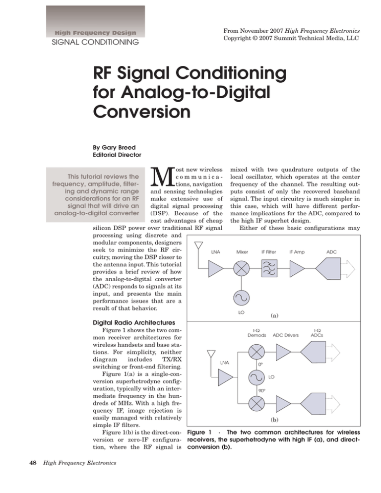
From November 2007 High Frequency Electronics Copyright © 2007 Summit Technical Media, LLC High Frequency Design SIGNAL CONDITIONING RF Signal Conditioning for Analog-to-Digital Conversion By Gary Breed Editorial Director M ost new wireless communications, navigation and sensing technologies make extensive use of digital signal processing (DSP). Because of the cost advantages of cheap silicon DSP power over traditional RF signal processing using discrete and modular components, designers seek to minimize the RF cirLNA cuitry, moving the DSP closer to the antenna input. This tutorial provides a brief review of how the analog-to-digital converter (ADC) responds to signals at its input, and presents the main performance issues that are a result of that behavior. This tutorial reviews the frequency, amplitude, filtering and dynamic range considerations for an RF signal that will drive an analog-to-digital converter mixed with two quadrature outputs of the local oscillator, which operates at the center frequency of the channel. The resulting outputs consist of only the recovered baseband signal. The input circuitry is much simpler in this case, which will have different performance implications for the ADC, compared to the high IF superhet design. Either of these basic configurations may Mixer LO IF Filter IF Amp ADC (a) Digital Radio Architectures I-Q I-Q Figure 1 shows the two comDemods ADC Drivers ADCs mon receiver architectures for wireless handsets and base stations. For simplicity, neither diagram includes TX/RX LNA 0º switching or front-end filtering. Figure 1(a) is a single-conLO version superhetrodyne configuration, typically with an inter90º mediate frequency in the hundreds of MHz. With a high frequency IF, image rejection is easily managed with relatively (b) simple IF filters. Figure 1(b) is the direct-con- Figure 1 · The two common architectures for wireless version or zero-IF configura- receivers, the superhetrodyne with high IF (a), and directtion, where the RF signal is conversion (b). 48 High Frequency Electronics High Frequency Design SIGNAL CONDITIONING have dual signal paths for diversity (MIMO), and may have much more complex front ends for multi-band, multi mode operation. Both types of receivers must deliver an appropriate signal to the ADCs if full performance is to be achieved. ADC Performance Considerations Any implementation of an ADC must consider the following performance factors: Amplitude range—The analog input range of an ADC is defined by the number of bits of resolution. The effective noise figure of an ADC is defined as the amplitude that will step the output from null (all bits “0”) to one LSB (least significant bit). Any lower level will not result in an output word other than null. Portions of the circuit preceding the ADC should not degrade system noise figure below that of the ADC. At the other extreme, the maximum signal level is that which just steps the output to all bits “on” or logical “1s.” A higher level will cause no change in the digital output. The IF amplifier in Fig. 1(a) or the ADC drivers in Fig. 1(b)—and possibly the LNA—should have gain control feedback (AGC) to maintain the signal at a level that does not exceed the fullscale ADC input. (Even if that input level is from an interferer rather than a desired signal.) Between the amplitude extemes, additional considerations for ADC performance include distortion and spurious response. Spurious signals can be distortion products, but they may also include clock feedthrough and quantization errors if the ADC does not have sufficiently good performance in these areas. Input bandwidth and clock rate— An ADC’s bandwidth is established at no more than one half the clock rate, the “Nyquist frequency.” However, harmonics of the Nyquist frequency may be used if the input bandwidth of the ADC is wide enough. This is undersampling, 50 High Frequency Electronics which is commonly used in high-IF wireless systems. Note that the input bandwidth remains at half the sampling frequency, even if the input frequency is much higher. In the direct-conversion architecture, there is no IF filtering to remove out-of-band signals. This means that on-frequency input filtering must provide some selectivity, and the ADC dynamic range must handle any remaining strong interfering signals. Only recently has ADC technology reached the point where dynamic range is sufficient to deliver base-station quality performance in a directconversion architecture. (Note: This is an important step foward for practical software-defined radios in all applications, not just consumer wireless.) Phase Noise and Jitter—Phase noise in a local oscillator is a wellknown issue to RF engineers, but the equivalent digital issue, jitter, may be a new concept. The ADC’s clock performance is just as important as the LO’s. Jitter is a time function, so its effect is frequency-dependent. In undersampled systems, the clock is effectively multiplied, which also multiplies the jitter. Even a low-jitter system (<0.2 psecrms) can have a power spectral density due to jitter alone that is 15 dB or more higher than the thermal noise floor. Whether this is a problem or not depends on system bandwidth and signal-to-noise requirements. There are other implications of jitter, including its contribution to quantization errors. Further reading is highly recommended. Circuit Implementation—General circuit design and construction techniques have the potential for serious problems in ADC performance. First is the difficult combination of a sensitive analog input, and a digital output of 8 to 24 bits which swing from zero to 3 or 5 volts, with fast edges. Separating the analog and digital grounds is the first defense against self-interference from digital output to analog input. All ADC applications data include design recommendations. Next, the DC power input is referenced to ground and has a similar potential for problems. Voltage regulation, bypassing and decoupling, and circuit layout all need to be executed properly to maintain a stable voltage at the DC supply pin. Additional layout issues involve signal paths external to the ADC device, including LO radiation, crosstalk from other digital signals within the system MPU or DSP circuits, display circuitry, keypad scanning signals, etc. With so much digital content in modern wireless equipment, there are a large number of opportunities for self-interference via small-signal RF paths. Summary RF/microwave engineers need to understand the nature of the analogto-digital conversion process when designing the circuitry that delivers the analog signal to the ADC input. They also need to be aware of the effects of digital circuitry, both in the ADC and elsewhere in the system. Digital specialists must appreciate the imperfections and uncertainties of analog signals. They need to understand factors such as noise, distortion and dynamic range. References 1. “The Care and Feeding of High Performance ADCs; Get All the Bits You Paid For,” Application Note 71, Linear Technology, www.linear.com 2. “Dynamic Performance Requirements for High-Performance ADCs and RF Components in Digital Receiver Applications,” Application Note 3062, Maxim Integrated Products, www.maxim-ic.com 3. “Effects and Benefits of Undersampling in High-Speed ADC Applications,” Article Reprint and Application Note, National Semiconductor, www.national.com 4. “Sampled Systems and the Effects of Clock Phase Noise and Jitter,” Application Note AN-756, Analog Devices Inc., www.analog.com
