Off-line application of the fixed frequency clamped mode series
advertisement
OFF-LINE APP1,ICATION OF THE FIXED FREQUENCY
CLAMPED MODE SERIES-RESONANT CONVERTER. *
J.A.Sabat6 ant1 F.C.1 ce
Virginia I'owrr Iilrctronics Center
Virginia I'olytccl~nicInstitutc arid Stale liniversity
Blacksburg, Virginia 24061
ABSTRACT
The performance of the clamped-mode series rcsotxmt ronverter
is studied for an off-lie application. Prototypes wcrc ticsigned for
operation below and above resonant frequency and zero-current turnoff or zero-voltage turn-on switching conditions. Ilieorctical characteristics are used for the design in each mode and the corresponding
region of operation is defined and verified expcrimentnlly. Main
sources of loss are identified.
1. INIRODUCTION
The clamped-mode series resonant converter provides tlic atlvnntagc of operating at a constant frequency while retaining most of the
desired features of conventional resonant converters. I'rcvious analysis
[1,2j of this converter shows that many different modcs o f operation
are possible and are defined according to the switching conditions of
the devices, namely, zero-current turn off or zero-voltage trirn on.
The purpose of this paper is to describe the design for selected
cases above and below resonant frequency and to measure their respective characteristics. The advantages and limitations o f cach opernting mode are assessed experimentally in terms of eficicncy and load
range.
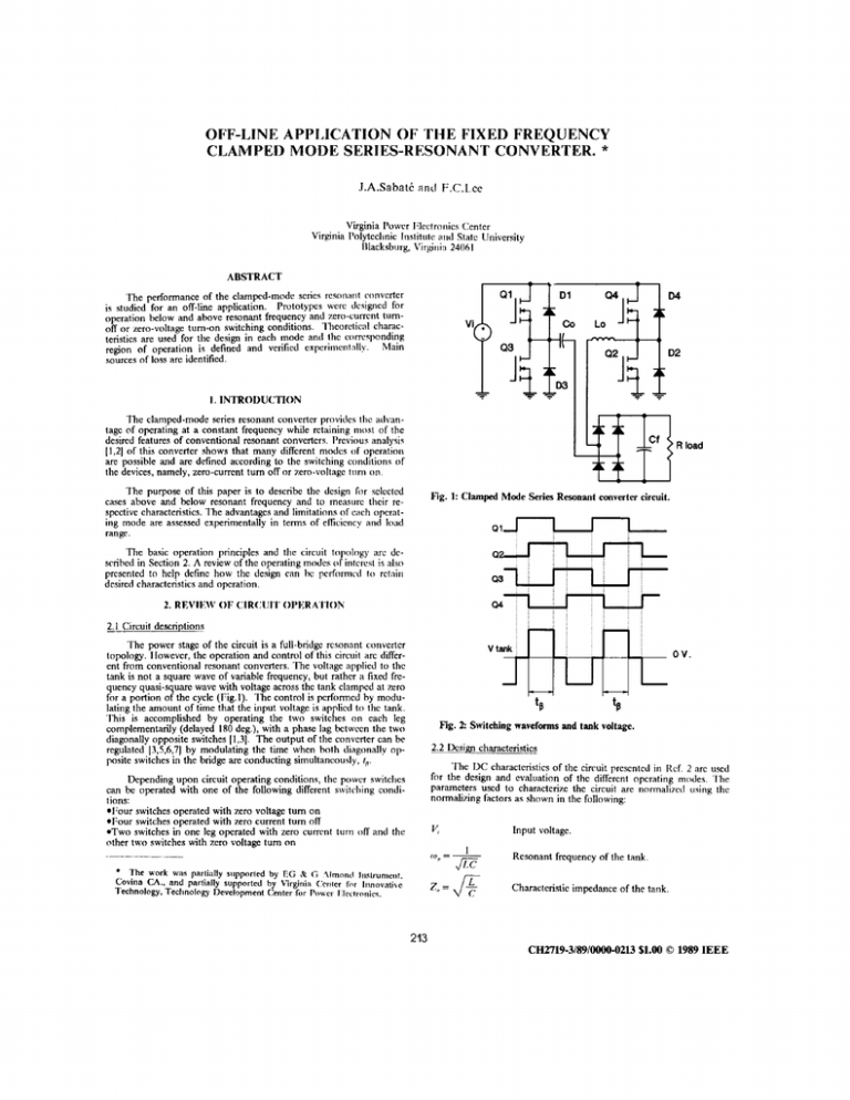
Fig. 1: Clamped Mode Series Resonant converter circuit.
The basic operation principles and the circuit topology arc dcscribed in Section 2. A review of the operating modes of infcrcst is also
presented to help define how the design can hc pcrformctt to retain
desired characteristics and operation.
2. REVIE\C' OF C I R C X J I I Ol'l~RA'l'lON
2.1 Circuit descriptions
The power stage of the circuit is a full-bridge rcsonnnt converter
topology. IIowever, the operation and control of this circuit arc different from conventional resonant converters. The voltage applied to the
tank is not a square wave of variable frequency, but rather a fixed frequency quasi-square wave with voltage across the tank clamped at zero
for a portion of the cycle (Fig.1). The control is performcd by modulating the amount of time that the input voltage is applicd to the tank.
'This is accomplished by operating the two switches on each leg
complementarily (delayed 180 deg.), with a phase lag bctwccn the two
diagonally opposite switches [1,3]. The output of the converter can be
regulated [3,5,6,7]by modulating the time when both diagonally 01'posite switches in the bridge are conducting simultaneously, 4.
Fig. 2: Switching waveforms and tank voltage.
2.2 Dcshharacteristics
~.
The IIC characteristics of the cirruit presented i n llcf 2 are used
for the design and evaluation of the different operating modes. 'I he
parameters used to characterize the circuit are normali7ctl using the
normalizing factors as shown in the following:
Depending upon circuit operating conditions, the powcr switclics
can be operated with one of the following different switching conditions:
*Four switches operated with zero voltage turn on
*Pour switches operated with zero current turn off
*Two switches in one leg operated with zero current turn off and the
other two switches with zero voltage turn on
v,
Input voltage.
1
<om= ___
JE
Ihe work was parlially slipported by EG & G 4lrnond Inalrunlellt.
Covina CA., and partially supported by Virginia ( h k r liw Innovatikc
Technology. Technology Development Center for Power 1:lccirorlir~.
.Z, =
213
&
Resonant frequency of the tank.
Characteristic impedance of the tank.
17
--L
b-
z,
Mode B
Base current.
2.3 Operation below resonant frequency
I
Q1
Considering the switching conditions of devices at n frcqucncy
below resonant frequency, the operation of the circuit can hc summarized in two basic modcs of operation whcn operating closc to resonance (Refs. [1,2]). The first mode is whcn the four active switches arc
turned off with zero current (mode A). The sccond is whcn two
switches turn off with zero current but, the other two switchcs turn o n
with zero voltage applied across them (mode 13).
Q2
03
1
1
r
I
Q4
&
r\
Shown in Figs.# 3 and 4 are waveforms corresponding to the tank
current and voltage as well as the capacitor voltagc. In I:ig.S, thc scquence of topological modes which the convrrtcr gocs through is tlrpicted .
In mode A (Fig. 3 ) , the currrnt passing through ilcviccs 1 and 2
changes direction while the two activc dcvices arc ( V I . Ilowrvcr. in
mode I3 the current does not reversc until after one of thc two active
devices has been turned off. This introduces another topological mode
in which the current is circl~latingwithin the tank, implying that two
of the switches turn off when current is circulating through tlicm. When
this topological mode occurs, the diode in parallel with the subsrquently conducting switch conducts prior to the power switch, allowing
the device to turn on with zero voltage applicd.
'B
Q3Q4b1 Q1 D4 Q 1 Q2 D3 D2Q3
Q4
Q2
Finally, another mode of operation has to be considcrcd, the discontinuous conduction mode. In this case the topological mode I l l , as
shown in Fig. 5 , does not occur. IIowever, the switching conditions
for the devices are qualitatively the same as in mode I3.
Fig. 4 Switching waveforms and tank voltage,mode B.
Mode A
The normalized load current is defined as:
Mode B
In Fig. 6, the I, vs. p angle is plotted. Each curve of thc figurc corresponds to a different normalized output voltage, defined as:
IV
In the DC characteristics, it can be observed that mode A is obtained
in a load range limited to higher I, above the dotted line in IGg.6, defined as Region A. Meanwhile, modes B and the discontinuous conduction mode cover a range of /,. from 0 to a maximum value of I,
dependent on V0,. Mode R operates in the region defined as Rcgion I3
helow the dotted line.
II
f+y0
0 2 D3
D1 D2
Lo
CO,.
Fig. 5 Topological modes below resonant frequency.
2.4Operation above resonant frequency
.-
In this case, two basic modes of operation are also cncountcred
(Pigs. 7, 8 and 9).
In mode A', the four active devices turn on with zero voltage. In
Fig.7, it can be seen that diodes D1 and D2 (or D3 and D4) are conducting until the current reverses, at which point MOSFl3's 01 and
4 2 (or Q3 and Q4) begin conducting. In the circuit this implies that
Q1 and Q2 ( 0 3 and Q4) turn on with zero voltagc. Ilowcvrr, the four
active devices turn off when Conducting current.
In mode B', the circuit operation goes through the same
topological modes (Fig.9) as in mode B, when it is below resonant
frequency. The switching conditions for the devices are the same as in
inode B. Two switches turn off with zero current ( 9 2 and 04) and thc
other two turn on with zero voltage. When conduction in mode 111
(Fig.9) is not possible, the circuit then operates in a discontinuous
conduction mode. The two switches that turn off with zrro ciirrent are
also turned on with zero current.
214
Mode B
Normalized load current ( W n 4 . 8 )
e
->
(d
0
80
40
x)
80
loo
120
140
180
180
P (deg. 1
Q1 Q1Q2 Q2D3 D2 Q3Q4 ~
Q3
D4
Fig. 6 DC characteristics below resonant frequency.
'l'ho I)(: characlcristics I,,,, W. /Ifor difkrcnt I Lr, arc s h o w in
Fig.10. Mode A' occurs for I,, almvc Ihc tlotlcJ linc in I;ig. IO, anti
modcs I3' and discontinuous conduction occur for lower v:llucs of I,,,
helow thr dottrd line in I5g. IO.
Fig. 8: Switching waveforms and tank voltage,mode B'.
3.2 Modes of in=
One of the main advantages of the resonant convcrtcr is that thc
sinusoidal nature of current and voltages reduccs switching losses, allowing the converter to operate at higher frcqucncics and powcr density.
3. I)@SI<;N CONSII~I~KA'I'IONS
3.1 I h i B objectives
The operation frequency of the converter is chosen to achicvc the
dcsiied power handling capability. The maximum powcr which can
be delivered to the load is not bound for an ideal tank. Ilowcvcr, in thc
actual tank, the parasitic losses of the components imposc a practical
limit on the maximum power obtainable. This is due to thc fact that,
when thc operating frequency gets closer to the resonant frcqucncy, thc
high values of current through the tank causes the losscs to incrcase
dramatically 141. Values of 0.8 and 1.2 times the rcsonant frcqucncy
were chosen for the design above and below resonant frcqucncy. This
decision is a compromise between power handling and elliciency, based
on previous studies of resonant converters (4).7besestudics show that,
for the quality factors attainable in the resonant tank, thc I)(' characteristics do no! differ significantly from thc ideal.
The design objectives for thc prototypes W C I C drfincd uiith an input voltage suitable for off-line application (between 200 and .IO0 \'.)
and an output power of 100 W for 5 V. Isolation betwccn input and
output is also desired for an off-line application.
The operating modes for the convertcr are chosen according to the
formerly-stated objectives and two modcs of opcration arr cxplored.
Mode A
Mode A'
Mode B'
IV
.
.
.
.
4
.
VQ
D3D4
43D2
Fig. 9:Topological modes above resonant frequency.
215
~
1
"15
Normalized load current (Wn=l . 2 )
SRSIM
Lo
%:I
rusM14oc
,
Fig. 11: Circuit below resonant frequency.
0
20
40
60
a0
loo
120
140
160
= 110
, deg. in Rcgion 13, a value
In order to have /Irn
Von(rnrx)
= 0.8 is chosen.
180
P (deg. 1
then,
Fig. 1 0 DC characteristics above resonant frequency.
Of thc possiblc choices, one ahoce rcsonancc and :iitothcr I d o w
resonancc wcre chosen for the prototypes.
and
3.3 Design below resonant frequency
Vo*min)
= 0.55
Two different modes of operation are possiblc for opcration below
the resonant frequency. From the point of view of eficiencq, inodc A
initiallv seemed to be attractive, but because the four diodcs arc forced
to turn off when there is current through thcm, their revrrsc rccovcry
characteristic produces signifcant turn-on losses in the active drviccs.
In addition, this mode is only attainable for a limitcd rangc of output
current and, for light loads, the converter will enter into nicitle I3 opcration.
the characteristic impedance is then,
The operation region is depicted in Pig. 12.
Normalized load current ( W n 4 .8)
Due to the former considerations, mode B was choscn to design
a prototype below resonant frequency. In this case, sincc two diodcs
are naturally commutated, the internal diode of the MOSI~IYI'scan be
used, reducing the component count. Also, lossless snubbcrs can hc
used for the two switches which are turned off with current, bccausc
these two switches turn on when zero voltage is applicd. 'I'hc circuit can
operate for full range of load with the same switching conditions.
1.0
,
Isolation is achieved by using a transformer with its primary in
series with the resonant circuit. The transformer is built with a center
tappcd secondary, in order to reduce the losses of the full wave output
rectifier. The complete power stage used is shown in rig. 1 I .
The following normalized parameters are used:
where n is the turns ratio between the primary winding and secondary
winding of the transformer, and Vsecis the voltagc in the half secontiar)
of the transformer Vsec= 5 V,,,,, and
0
20
40
80
80
ml
tP
740
180
(00
B (deg.1
+
Fig. 1 2 Operation region below resonant frequency
3.4 Design above resonant frequency
where 20 A is the nominal output current.
Above the resonant frequency, two modes of operation arc possible. Mode B' works in the same way as mode n, which was used for
the design below resonant frequency. In mode A', the four active
switches turn on without voltage being applied across thcm (which
seems to be most attractive for higher frequencies). In addition. the
In order to operate in the forced commutation mode, the maximum value of fori, cannot exceed a certain value. Mode n occurs helow
the dotted line in Pig. 6 A value Iodm8x)
= 0.9 is choscn.
216
four diodes turn off naturally, meaning that fast rccovcr)' diodes arc not
required and the internal diodes of the MOS1:RI's can bc uscd.
Normalized load current (wn-1 .2)
'l'he secondary circuit is the same as for the case below resonant
frequency. The complete circuit is shown in Fig. 13.
The design procedure, considering now the DC char;\cteristics of
Pig. 10, is the following:
Vd.85---
Given a maximum p angle of operation of 150 dcg. Por a valuc of
= 1.1, in order to avoid modc B' and ensure regulatioll at maximum p, lon(m.x)
is chosen as,
then at full load,
l'he maximum power transfer is achieved for V,, = 0.5 141, thcn this
value is chosen for Von~max),
hence Vonlon(min)
= 0.35.
o
40
x)
do
m
io0
120'
140
iw
im
B (deg.)
and
Fig. 1 4 Operation region above resonant frequency
Z,=
l'he characteristic impedance is calculated as
4. EXPERIMENTAL RICSU1,'I'S
Q.
Shown in Fig. I5 are the ideal DC characteristics and the measured points on the prototype. The measurements are in rcasonablc
agreement with the expected results.The discrepancies arc due to the
finite Q of the tank and the switching losses of the MOSI:IYl's.
4.1 Below resonant frequency
The values fbr the circuit used in the prototype are: II = 20 turns,
C = 1.16nF, L = 7 9 p l I , where,l,=I,~+L,~=69/1/1+I O \ i / l . I'hesc
values and w , = w, / UI,, = 0.8 give:
&
= 261
The MOSFETs used were lRP730, which can block 400 Volts
and have a channel resistance of 1 51. 'The external diodes arc fast rccovery diodes (r,, = 30 nsec) . The serial diodes, which arc usctl to avoid
conduction of the internal diodes of the MOSPEl's, arc Schottky diodes (SRS02). The rectifying diodes are also Schottky diodes
(IJSM l40C), used to reduce rectifying losses.
The operation region is shown in Fig. 14 for an input range of
between 200 and 300 V. and load range between 20 A and 12.5 A.
fo=--
&
Waveforms of voltage and current in the tank are shown in IGgs.
16 and 17 for the low and high lime (200 and 300 V), respcctivcly.The
noise observed on the current waveform is mainly due to thc rcrovery
of the diode.
- 525 kllz
A = 0.8 x f . = 420 k l l z
Shown in Fig. 18 are the current and voltage of one of the
MOSFETs which turns off with zero current. A high pcak of current
is observed during the turn on. This causes the switching losscs to increase and the efficiency to be lower than expected.
I
4.2 Above resonant frequency
"' +
The values for the circuit used in the prototype arc: 17 = I 8 turns ,
C = l . l n F , L = 103p11, w h e r e , l = L , + L , ~ = 9 5 ~ i I I + X ~ i / 1thcsr
,
values and
w, = w,
/
U),
=
1.2 , give,
1
f.= = 413 kllz
JE
1; = 1.2 x f , = 561 kHz
Ze =
fi
= 306 51
The DC characteristics used for the design have bccn verified, and
the agreement with the measurements is reasonable. Whcn the Q of the
resonant tank is too far from ideal, possible deviations in the design
should consider to avoid not covering the desired operating area. This
becomrs particularly critical when it is closc to maximum fi angle.
loed
..
Fig. 1 3 Circuit above resonant frequency.
217
Normalized av . current , w n 4 .8
Fig. 1 7 Waveforms below resonant frequency (low line).
(Scale: vert. 100 V/div. and 0.5 A/div
hor:500 nsec./div.)
o
20
40
do
m
~ 1 0 1 2 0 i a i m i o
The measured points are plottcd togcther with the iilral characteristics in Fig. 19. The deviation from ideal characterisiics increases
with fi, as the slope of the characteristics decreases. Due to the deviation from ideal behavior, a maximum current of 18.5 A was obtained
for low line, instead of 20 A, for the maximum fi angle ( I 50 deg.).
B (deg.)
Fig. 15 Measurements below resonant frequeiicy
Shown in Figs. 20 and 21 are the oscilloscope waveforms for high
and low line at full load.
4.3 Efficiency measurements
The efficiency at different operating points was mcasurctl for both
prototypes and the results plotted in Figs. 22 and 23.
The evaluation of losses is given in Table I (Fig.24). 'I'hc losscs in
the rectifiers are the most significant in an cases (for 5 V. output). Sincc
the external diodes (D2 and D4,Fig. 11) are turned off with high current
and high reverse voltage, the turn-on losses of MOSITI's U 2 and 0 4
are very high, and the switching losses become significantly liighcr than
in the other cases.
Above resonant frequency, the maximum and minimum values
of V,, chosen in the design are lower than for below rcsonant frcqriency. These lower values of V, (0.35 and 0.5) were choscn to provide a larger load range (Figs.10 and 14). Smaller valucs for I/, imply
a lower transformer turns ratio (18 instead of 29), resulting in a highrr
primary current (tank current) for the same output p w c r . Consequently the conduction loss becomes more significant than for the
prototype which works below resonance (6.5 and 3.5 watts vs. 2.5 and
2.1 watts)
Fig. 1 6 Waveforms below resonant frequency (high line).
(Scale: vert: 100 V/div. and 0.5 A/div
hor:500 nsec./div.)
Fig. 18: Switching waveforms. Left zero current turn off,
right zero voltage turn on.
(Scale: vert: 100 V/div. and 0.5 A/div
hot500 nsec./div.)
218
Comparing the overall performance, the casc with ftwr switches
turned on with zero voltage (above .resonant frcqucncyj xhievcs a
better efficiency while operating at higher frequcncies. I lowcver.,i n the
case above resonant frequency, full load range is not attainahlc in mode
.
Normalized av current , wn=l . 2
A'.
The load range is rather narrow in Region A' (abovc resonant
frequency) for high input line (300 V). At a load of 18 A. (with 300
V. input) the converter is operating on the boundary bctwccn Regions
A' and B' and, consequently, two of the switches do not turn on with
zero voltage. Examining the loss breakdown in Table I, it can be s e n
that for a load of 18 A., the switching loss is considerably higher than
for a load of 2.5 A.
80
o
a0
U
w
w
100
iao
IU
im
75
70
iw
B(deg.)
Fig. 19: Measurements above resonant frequency.
65
%O
55
50
45
40
0 2 4 6 8 10 12 14 16 1820
lout
Fig. 2 2 Efiiciency below resonant frequency.
90
Efficiencv Wn=l .2(measured)
Fig. 20: Waveforms above resonant frequency (high line).
(Scale: vert: 100 V/div. and 0.5 A/div
hor:500 nsec./div.)
80
70
96
60
50
40
Fig. 23: Efiiciency above resonant frequency.
fig. 21: Waveforms above resonant frequency (IOW tine).
(Scale: v e r t lo0 V/div. and 0.5 A/div
hoc500 nsec./div.)
219
Two prototypes were designed and tcsted expcrimcnktlly, one to
operate in Region R below resonant frequency and thc othcr to opcrate
in Region A’ above resonant frequency.
The efficiency is mainly determined by the rectifier loszcs and the
switching losses. In the case where the mode B of opcration is implemented (below resonant frequency), the recovery of thc diodes increases the turn-on losses of the devices dramatically. ‘l’hc operation
mode with four switches turned on at zero voltage, modc A’ at above
resonant frequency, shows better efficiency. Therefore, if higher frequencies of operation are desired, mode A’ is the better choicc among
the four modes of operation discussed in the paper.
6. REFERENCES
Fig. 2 4 TABLE I: Evaluation of losses.
P.S.T’sai, P.Matcru and F.C.Lec.“Constant I;rcqucncy,
Clamped Mode Resonant <:onvcrtcrs.”ll:I~I: procecdings
PES(: 1987.
5. CONCLIJSIONS
The Clampcd Mode Series Resonant Convericr (C$,lSl<C) opcrates at a fixed frequency with the devices turned on with zero voltagc
or turned off with zero current. In addition to good switching conditions, the CMSRC has the advantage of fixed frequency oprration, rcsulting in an easier design of magnetic components for rcsoiiant tank
and filtering. This study has proved that it is fcasihlc t o use thc
CMSRC at a fixed frequency for an off-line application.
F.S.‘Isai and F.C.lxe.“Cornplete 1IC characterization o f
Constant Frequency Clamped Mode Scricv Rcsonant
Converter.”lEEE proceedings PIISC 1988.
.I.I’itel.“Phase-modulated Resonant Power (‘onversion
Techniques for high frequency inverters.”ll:l;li I A S annual
meeting 1985.
The clamped mode operation at a fixed frequency o f thc scrics
resonant converter presents a different mode of operation when the
switching frcquency is either above or below the resonant frcqucncy:
Below resonant frequency, either four devices are turnctl off with zcro
current (mode A), or two are turned off with zero current arid two arc
turned on with zero voltage (mode R and discontinuous conduction).
Above resonant frequency, either four active devices arc turned on
with zero voltage (mode A’), or two are turned on with zcro voltagc
and two are turned off with zero current (modes l3’ and diwontinuous
conduction).
R.Oruganti.“State plane analysis of rcsonant convcrtcrs.”
PhD. dissertation , Virginia I’olytechnic Instil iilc and Statc
IJniversity March 1987.
P.S.Tsai.“Constant
Frequcncy
Resonant
power
processors.” M.S. Thesis, Virginia I’olytechnic Institute and
State Ilniversity, 1985.
P.Materu and P.C.I~e.“Constant-Prcqucnc~Rcsonant
Converter.” Annual report EG & G Almontl Instrument.
1986.
The IIC characteristics have been used for the dcsign. Ahovc resonant frequency, two regions of operation are defined:
Region A’, for large values of I,, where the convcrtcr opcratcs in
mode A‘ and Region H’, between no load and the boundary with Region A’, where the converter operates in mode l3’ o r tliscontinuous
conduction mode.
Below resonant frequency two regions of opcration itrc tlcfi~icd:
Region A, where the converter operates in modc /\, th:lt occurs for
large values of I,, and Region B, where the convertcr opcratcs in inode
B, that ranges between no load and the boundary with Rcgion A .
Yuan Chin.“Constant frequency Parallel resonant Converter.” M.S. Thesis, Virginia Polytechnic lnstitutc and
State University, 1986.
Juan A. Sabate.“Clamped-Mode Fixed-frequcncy Series
Resonant Converter , off-line application: Analysis and
Implemcntation.” M.S. Thesis, Virginia Polytechnic Institute and State University, 1988.
220
