Final Exam review Solution
advertisement
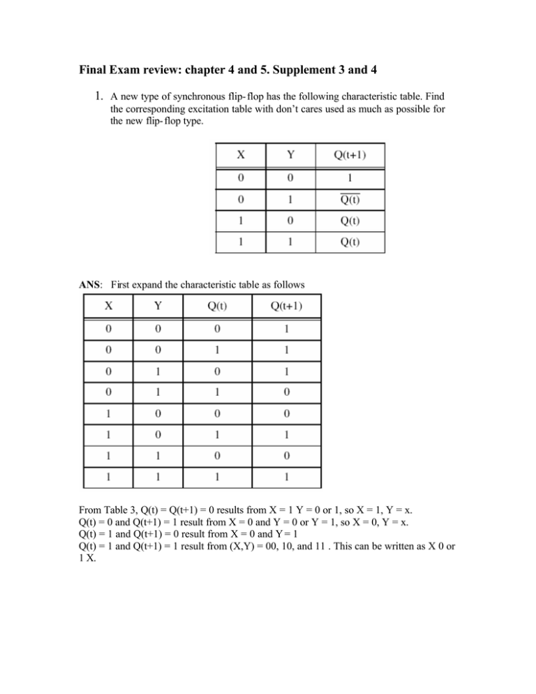
Final Exam review: chapter 4 and 5. Supplement 3 and 4 1. A new type of synchronous flip- flop has the following characteristic table. Find the corresponding excitation table with don’t cares used as much as possible for the new flip- flop type. ANS: First expand the characteristic table as follows From Table 3, Q(t) = Q(t+1) = 0 results from X = 1 Y = 0 or 1, so X = 1, Y = x. Q(t) = 0 and Q(t+1) = 1 result from X = 0 and Y = 0 or Y = 1, so X = 0, Y = x. Q(t) = 1 and Q(t+1) = 0 result from X = 0 and Y = 1 Q(t) = 1 and Q(t+1) = 1 result from (X,Y) = 00, 10, and 11 . This can be written as X 0 or 1 X. Therefore, the excitation table for XY flip- flop is 2. A state table is given along with an assignment of binary codes to the states. (a) In the blank Table A provided, find the state table with the states and next states represented by their binary codes. (b) In the blank Tables B provided, fill in the required D inputs to implement state variable A using a D flip- flop and J and K inputs to implement state variable B using JK flip- flops. Be sure to show the don’t cares for J and K. (c) Find (and write in Table C) the minimum cost sum-of-products equations for the D input for flip-flop A and for the J and K inputs for the flip- flop B. 3. The clock "CLOCK" signal shown graphically below is tied in common to five different, single-bit flip-flops (or latches). The "A" signal is tied to the "D", "T", "J" inputs of any D, T, or JK flip-flop (or latch) respectively. The "B" signal is tied to the "K" inputs of any JK flip- flop (or latch) respectively. The "Q" outputs of these different flip-flops (or latches) are shown as signals W1, W2 and W3 Assume that the clock period is MUCH LONGER than the clock to output delay of the flip- flops or latches. For each row in the table below, mark an "X" in the column for the waveform if that waveform is possible for the flip- flop listed. If none of the waveforms fit the flip- flop type, mark an "X" in the column labeled "NONE". 4. Sequence Recognizers, Moore and Mealy Models and ASM Charts. (a) The State Diagram to the right recognizes an input sequence pattern. What is it? ANS: 101 (b) The sequential machine model described by the state diagram is (circle the CORRECT one): ANS: (c) In the space below, draw an ASM chart EQUIVALENT to the State Diagram above. LABLE all states, inputs, and outputs consistent with the above State Diagram. 5. Design a serial parity-bit generator_ Assume the input x is received sequentially_ The parity bit generator will convert every third bit of the input sequence to the even parity bit of the first two bit. For example, if the inputs are 11b01b10b00b… where b denotes don’t cares, then the corresponding outputs are 110011101000… where the parity bits are in red. The state diagram has 5 states, A, B, C, D, and E, as shown below. Label on each arc the corresponding input and output. You may use b as one of the input symbol to represent don’ t care. ANS: 6. A toggle flip-flop's characteristic table is as follows: A sequential circuit contains exactly one T flip- flop. If the flip-flop input equation is T(t) = AB + Q(t)B where A(t), B(t) are input variables to the sequential circuit. Find the next state equation of that sequential circuit in the minimum SOP standard format. ANS: Substitute T(t) into characteristic equation Q(t + 1) = Q(t) ⊕ T(t), we have Q(t + 1) = (AB’ + QB)Q’ + (AB’ + QB)’Q = AB’Q’ + A’B’Q 7. A state-of-the art microprocessor has a clock frequency of 2GHz (2 x10⁹ cycles/second) (a) What is the clock period for the microprocessor in nano (10-9) seconds? ANS: 0.5 ns (b) Timing parameters are given for the flip- flops in the Table below. What is the maximum time delay that can be tolerated for a combinational logic path from flip- flop to flip- flop in the microprocessor? ANS: CP = time delay + tp + tsu => time delay = CP - tp - tsu = 0.5 - 0.1 - 0.05 = 0.35 ns 8. A circuit shown below will be analyzed for maximum clock rate. Assume that the circuit has been minimized. All gates and flip flops implementing the circuit have the following timing parameters: (a) What is the minimum clock period for the circuit to ensure it will function properly? ANS: 4 (b) What is the minimum clock period for the circuit to ensure it will function properly? ANS: 8 + (4x7) + 4 = 40 ns 9. Construct a BCD down counter by connecting together the given components and labels: 10. Assuming the circuit below begins in state 0,0,0, write the sequence of states that occurs in the boxes given below the flip-flops. 11. Four positive edge-triggered flip- flops with asynchronous clear are shown. Connect the flip- flops and additional logic to form a synchronous binary up counter (counts 0, 1, 2, …,15, 0, ...). This counter has an ENABLE input. With ENABLE = 1, the counter counts up. With Enable = 0, the counter holds its current value. The additional logic is to consist ONLY of AND gates with as many inputs as needed and the type of gating is to be PARALLEL (not SERIAL) to permit a high clock frequency. 12. A synchronous binary counter is given below along with a quad two-way multiplexer. The binary counter has a synchronous LOAD and a synchronous RESET. Q3 is the most significant bit of the counter and Q0 is the least significant bit. Add constant values to the data inputs to the multiplexer and combinational logic to the multiplexer select input S, the counter input LOAD, and the counter input RESET to generate the following sequence of counts: 0, 1, 2, 6, 7, 8, 12, 13, 14, 0, ... 13. The block diagram of a special shift register is given below. This register is controlled by a 2-bit code (S1, S0) with the operations performed listed in the table below. In the right rotate, the leftmost bits are filled with the bits falling out on the right, e.g., for a right rotates of 2 positions, 01110010 become 10011100. In the left shift, the vacated rightmost bits are filled with 1’s. Manually simulate the register for 8 clock cycles with the initial contents and inputs as given in the simulation table below. The results due to any given line of the table are to appear on the following line due to the positive clock edge triggering of the register. 14. Design a 4-bit shift register that performs the following operations based on the 2-bit control input SC(1:0). Neatly draw your design using the ip-ops given below. On the left of the page draw logic that serves all cells, if any is needed. 15. Using the synchronous binary counter of figure 5-12 and an AND gate, construct a counter that counts from 9 to 69. Add an addition input to the counter that initialized it synchronously to 9 when the signal INIT is 1. 16. A combinational circuit is a direct realization of the switching function: f = a’c + ad + ab’ . The circuit is a two- level AND-OR circuit with inverters at the input to generate a and b. All gates and inverters have a delay of 1ns. (a) Can a single input change cause a static-1 hazard in this circuit? If yes, identify a single input change that causes a static-1 hazard. Use a Karnaugh map to demonstrate the static-1 hazard you have identified. ANS: Yes (b) Can a two input change cause a 0- functional hazard in this circuit? If yes, identify 2 examples of two input change tha t causes a 0-functional hazard Use a Karnaugh map to demonstrate the 0- functional hazard you have identified. ANS: Yes (c) What additional gates must be included in this circuit to eliminate all static-1 hazards without changing its function (obviously). Show the additional gates on a Karnaugh map instead of drawing a logic diagram. ANS:
