iT2008
advertisement

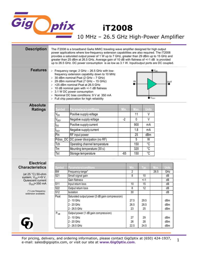
iT2008 10 MHz – 26.5 GHz High-Power Amplifier Description Features Absolute Ratings Electrical Characteristics (at 25 °C) 50-ohm system, VDD=+9 V, Quiescent current (IDQ)=350 mA (*) Low frequency extension available. The iT2008 is a broadband GaAs MMIC traveling wave amplifier designed for high output power applications where low-frequency extension capabilities are also required. The iT2008 provides a saturated output power of 1 W up to 7 GHz, greater than 29 dBm up to 15 GHz and greater than 25 dBm at 26.5 GHz. Average gain of 10 dB with flatness of +/-1 dB is provided up to 26.5 GHz. DC power consumption is as low as 3.1 W. Input/output ports are DC coupled. ¾ Frequency range: 2 GHz – 26.5 GHz with lowfrequency extension capability down to 10 MHz ¾ 30 dBm nominal Psat (2 GHz – 7 GHz) ¾ 29 dBm nominal Psat (7 GHz – 15 GHz) ¾ >25 dBm nominal Psat at 26.5 GHz ¾ 10 dB nominal gain with +/-1 dB flatness ¾ 3.1 W DC power consumption ¾ Nominal DC bias conditions: 9 V at 350 mA ¾ Full chip passivation for high reliability VDD IN OUT VGG1 Symbol VDD Parameters/conditions Positive supply voltage Min. Max. 11 Units V VGG1 Negative supply voltage -2 0 V IDD Positive supply current 900 mA IGG1 Pin Pdiss_DC Tch Tm Tst Negative supply current RF input power DC power dissipation (no RF) Operating channel temperature Mounting temperature (30 s) Storage temperature 1.8 25 5 150 320 150 mA dBm W °C °C °C Symbol BW S21 S11 S22 S12 Psat P1dB -65 Parameters/conditions Frequency range* Small signal gain Gain flatness Input return loss Output return loss Isolation Saturated output power (3 dB gain compression) 2 - 10 GHz 2 - 20 GHz 2 - 26.5 GHz Output power (1 dB gain compression) 2 - 10 GHz 2 - 20 GHz 2 - 26.5 GHz Min. 2 8 10 8 30 Typ. 10 +/-1 15 12 Max. 26.5 Units GHz dB dB dB dB dB 27.5 26.5 23 29.5 28.5 25 dBm dBm dBm 27 26 22.5 29 28 24.5 dBm dBm dBm For pricing, delivery, and ordering information, please contact GigOptix at (650) 424-1937, e-mail: sales@gigoptix.com, or visit our site at www.GigOptix.com. 1 iT2008 10 MHz – 26.5 GHz High-Power Amplifier Thermal Characteristics Symbol Rth_jb Rth_jb Parameters/conditions Rth_jb (oC/W) Tch (oC) Thermal resistance junction-back side of die No RF: DC bias VDD = 9 V, IDQ = 35 0mA , PDC = 3.1 W 9.2 98.5 Tbase = 70 C Thermal resistance junction-back side of die RF applied: Saturated power 1 W, VDD = 9 V, Pdiss = 4.4 W 9.2 110.6 Tbase = 70 C MTFF (h) >> +1E7 >> +1E7 Chip Layout and Bond Pad Locations (Back of chip is RF and DC ground) P6 P5 P4 P1 P2 P3 Chip size tolerance: ± 20 µm Chip thickness: 4 mil with a tolerance of ± 0.4 mil. Pinout and pad dimensions: P1: RF input (100 x 150 µm2) P2: VGG1, negative voltage (100 x 100 µm2) P3: Gate low-frequency extension (250 x 100 µm2) P4: RF output and Vdd bias (option 2) by means of bias-tee (100 x 150 µm2) P5: Drain low-frequency extension (300 x 100 µm2) P6: VDD positive voltage (option 1) by means of choke (200 x 100 µm2) Note: All dimensions are in millimeters For pricing, delivery, and ordering information, please contact GigOptix at (650) 424-1937, e-mail: sales@gigoptix.com, or visit our site at www.GigOptix.com. 2 iT2008 10 MHz – 26.5 GHz High-Power Amplifier Input Return loss, VDD = 9 V, IDD = 350 mA 20 18 16 14 12 10 8 6 4 2 0 -2 -4 -6 -8 -10 10 5 0 -5 -10 S11 (dB) S21 (dB) Performance Data, T = 25 °C Small Signal Gain, VDD = 9 V, IDD = 350 mA -15 -20 -25 -30 -35 -40 -45 -50 2 4 6 8 10 12 14 16 18 20 22 24 26 28 2 4 6 8 10 12 Freq. (GHz) 12 8 4 0 -4 S21 (dB) S22 (dB) -8 -12 -16 -20 -24 -28 -32 -36 -40 4 6 8 10 12 14 16 18 16 18 20 22 24 26 28 Gain vs. Drain Bias VDD, IDD = 350 mA Output Return loss, VDD = 9 V, IDD = 350 mA 2 14 Freq. (GHz) 20 22 24 26 28 Freq. (GHz) 20 18 16 14 12 10 8 6 4 2 0 -2 -4 -6 -8 -10 8V_350mA 9V_350mA 2 4 6 8 10 12 14 16 18 20 22 24 26 28 Freq. (GHz) Gain vs. Temperature, VDD =9V S 21 (dB ) 20 18 16 14 12 10 8 6 4 2 0 -2 -4 -6 -8 -10 Tbase=0C Tbase=25C Tbase=50C Tbase=70C 2 4 6 8 10 12 14 16 18 20 22 24 26 28 Freq. (GHz) For pricing, delivery, and ordering information, please contact GigOptix at (650) 424-1937, e-mail: sales@gigoptix.com, or visit our site at www.GigOptix.com. 3 iT2008 10 MHz – 26.5 GHz High-Power Amplifier P1dB, VDD = 9V, IDD = 350 mA Saturated Power, VDD = 9 V, IDD = 350 mA 40 38 36 34 32 30 28 26 24 22 20 18 16 14 P1dB(dBm) Psat(dBm) Performance Data, T=25 °C 2 4 6 8 10 12 14 16 18 Freq. (GHz) 20 22 24 40 38 36 34 32 30 28 26 24 22 20 18 16 14 2 26 6 8 10 12 14 16 18 20 22 24 26 Freq. (GHz) Output Third Order Intercept Point, VDD = 9 V, IDD = 350 mA P1dB vs. VDD, IDD=350 mA 60 40 38 55 36 34 50 VDD=9V 32 30 28 26 24 22 OIP3(dBm) P1dB(dBm) 4 VDD=8V 45 40 35 30 25 20 18 20 16 14 15 2 4 6 8 10 12 14 16 Freq. (GHz) 18 20 22 24 26 2 4 6 8 10 12 14 16 Freq. (GHz) 18 20 22 24 For pricing, delivery, and ordering information, please contact GigOptix at (650) 424-1937, e-mail: sales@gigoptix.com, or visit our site at www.GigOptix.com. 26 4 iT2008 10 MHz – 26.5 GHz High-Power Amplifier Recommended Assembly Diagram for 2 to 26.5 GHz Applications VDD (option 1) 100 uF RF Output and VDD (option 2) thru bias tee RF In VGG1 1. For applications at 2 GHz and above, only an inductor of Lc> = 3 nH (1 mil long bond wire >2.5 mm) is necessary to provide drain bias. 2. Bypass capacitor must be large enough to isolate bias supply (> = 10 µF) For pricing, delivery, and ordering information, please contact GigOptix at (650) 424-1937, e-mail: sales@gigoptix.com, or visit our site at www.GigOptix.com. 5 iT2008 10 MHz – 26.5 GHz High-Power Amplifier Recommended Assembly Diagram for 10 MHz to 26.5 GHz Applications VDD (option1) (1) RF output and VDD (option 2) thru bias tee RF input VGG1 1. Appropriate low-frequency choke must be applied for 10 MHz applications. For pricing, delivery, and ordering information, please contact GigOptix at (650) 424-1937, e-mail: sales@gigoptix.com, or visit our site at www.GigOptix.com. 6 iT2008 10 MHz – 26.5 GHz High-Power Amplifier Recommended Procedure for Biasing and Operation CAUTION: LOSS OF GATE VOLTAGE (VGG1 and VGG2) WHILE CORRESPONDING DRAIN VOLTAGE (VDD) IS PRESENT CAN DAMAGE THE AMPLIFIER. The following procedure must be considered to properly test the amplifier. The iT2008 amplifier is biased with a positive drain supply (VDD) and one negative gate supply (VGG1). The recommended bias conditions for the iT2008 is VDD = 9.0 V, IDD = 350 mA. To achieve this drain current level, VGG1 is typically biased between –0.7V and –0.9 V. The gate voltage (VGG1) MUST be applied prior to the drain voltage (VDD) during power up and removed after the drain voltage is removed during the power down. Drain bias VDD can be applied to the drain (P6). Alternatively, the positive power supply can be applied through an external bias tee to the RF Output pad (P4) . Low Frequency Operation Application Information External coupling capacitors are needed at the RF_IN (P1) and RF_OUT (P4) ports. The auxiliary gate pad (P3) and drain pad (P5) are provided to extend performance below 2 GHz. Connect these pads via large external capacitors to ground to maintain input and output VSWR at low frequencies. Do not apply bias to these pads. Two options are allowed to provide the positive drain voltage VDD. Option 1 uses an onchip pad (P6) where an appropriate value of inductance (choke) must be used to maintain good matching over bandwidth, as reported in the assembly diagram. Option 2 uses an external bias-tee directly from the pad at the RF output. For application as low as 10 MHz a large value of inductance must be used in parallel with appropriate resistors in order to optimize gain flatness. CAUTION: THIS IS AN ESD SENSITIVE DEVICE Chip carrier material should be selected to have GaAs-compatible thermal coefficient of expansion and high thermal conductivity such as copper molybdenum or copper tungsten. The chip carrier should be machined, finished flat, plated with gold over nickel and should be capable of withstanding 325° C for 15 min. Die attachment for power devices should utilize gold/tin (80/20) eutectic alloy solder and should avoid hydrogen environment for PHEMT devices. Note that the back side of the chip is gold plated and is used as RF and DC ground. These GaAs devices should be handled with care and stored in dry nitrogen environment to prevent contamination of bonding surfaces. These are ESD sensitive devices and should be handled with appropriate precaution including the use of wrist-grounding straps. All die attach and wire/ribbon bond equipment must be well grounded to prevent static discharges through the device. Recommended wire bonding uses 3-mil-wide and 0.5-mil-thick gold ribbon with lengths as short as practical allowing for appropriate stress relief. The RF input and output bonds should be typically 12 mil long corresponding to a typical 2 mil gap between the chip and the substrate material. For pricing, delivery, and ordering information, please contact GigOptix at (650) 424-1937, e-mail: sales@gigoptix.com, or visit our site at www.GigOptix.com. 7


