Designing robust asynchronous circuit components
advertisement
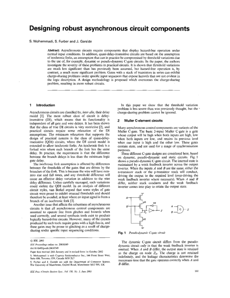
Designing robust asynchronous circuit components S. Mohammadi, S. Furber and J. Garside Abstract: Asynchronous circuits require components that display hazard-free operation under normal input conditions. In addition, quasi-delay-insensitive circuits are based on the assumption of isochronic forks, an assumption that can in practice be compromised by threshold variations due to the use of, for example, dynamic or pseudo-dynamic C-gate circuits. In the paper, the authors investigate the severity of these problems in practical circuits. It is shown that threshold variations are much less significant than has previously been assumed, but hazard-free operation is, by contrast_ a much more significant problem. Gates with a stack of transistors in series can exhibit charge-sharing problems under specific input sequences that expose hazards that are not evident in the Iogc description. A design methodology is proposed which overcomes the charge-sharing problem, resulting in more robust circuits. 1 Introduction Asynchronous circuits are classified by, inter alia, their delay model [I]. The most robust class of circuit is delayinsensitive (DI), which means that its functionality is independent of all gate and wire delays. It has been shown that the class of true DI circuits is very restrictive [2], and practical circuits require some relaxation of the Dl assumptions. The minimum relaxation that supports the design of practical systems is the class of quasi-delayinsensitive (QDI) circuits, where the D1 circuit model is extended to allow isochronic forks. An isochronic fork is a forked wire where each branch of the fork has the same delay. In practice, the requirement is that the difference between the branch delays is less than the minimum logic gate delay. The isochronic fork assumption is affected by differences between the thresholds of the gates that are driven by the branches of the fork. This is because the wire will have nonzero rise and fall times, and any threshold difference will cause an effective delay variation in addition to the wire delay difference. Unless carefully managed, such variations could violate the QDI model. In an analysis of different circuit styles, van Berkel argued that some styles of gate circuit were prone to exhibit unusual thresholds and should therefore be avoided. at least where an input signal is from a branch of an isochronic fork [3]. Another issue that affects the robustness of asynchronous circuits is that all asynchronous control components are assumed to operate free from glitches and hazards when used correctly, and several synthesis tools exist to produce logically hazard-free circuits. However, many of the circuits produced by such tools require gates with a high fan-in, and these gates may be prone to glitching as a result of chargesharing under specific input sequencing conditions. 0IEE. 2003 IEE hocerdings onPne no. 20030349 doi: 10.1049/ipcd~:~w3034~ Paper first received 281h January and in revised form 1st Oclobci 2002 S. Mohsmmildi is with C u ~ e n c yScmionducrui Inc.. 144 Fronl Slrccf West. Suite 600. Toionro, ON, Canada MSJ ZL7 S. Furbe? and J. Ganide am with the Department of Computer Science, The University of Manchsler, Oxford Road, Manchester M I 3 YPL UK IEE Proc-Cirruir.~Decices S v x V d 150, ,Ab 3, hr2e 2003 In this paper we show that the threshold variation problem is less severe than was previously thought, but the charge-sharing problem cannot be ignored. 2 % Muller C-element circuits Many asynchronous control components are variants of the Muller C-gate. The basic 2-input Muller C-gate is a gate whose output will be high when both inputs are high, low when both inputs are low, and retains its previous level when one input is high and the other low. These gates contain state. and are used for a range - of synchronisation purposes. Three different C-gate designs are considered here_ based on dynamic, pseudo-dynamic and static circuits. Fig. 1 shows a nseudo-dvnamic C-eate circuit. The intemal state is maintaiied by a Greak feedgaack inverter across the output inverter. When the inputs A and B are the same, either the n-transistor stack or the p-transistor stack will conduct, driving the output to the required level (over-driving the weak feedback inverter where necessary). When A and B differ, neither stack conducts and the weak feedback inverter comes into play to retain the output state. z "B. B Fig. 1 P.wdo-dyumic C-garr circuit The dynamic C-gate circuit differs from the pseudodynamic circuit only in that the weak feedback inverter is omitted. When A and B differ, the output state is retained as the charge on node 2,. The charge is not retained indefinitely, and the leakage characteristics determine the maximum time that the gate operates correctly when A and B differ. 161 In both the dynamic and pseudo-dynamic gates the noninverting output is used. The gate has a good output drive and the inputs pass through two inverting stages to reach the output. A static C-gate circuit is shown in Fig. 2. Active feedback is used to ensure that the output is driven in all the input states. and no over-driving is required in any input transition. Both the inverting and the non-inverting outputs may be uscd, with the former representing only a single inverting stage from input to output. Note that only the leftmost transistor stacks i r e important when switching Z,; the other stacks are used only for state holding. Fig. 3 shows the switching characteristics of node Z, of the three different circuits using 0.35 pm technology. The input is a very slow ramp starting just below the gate threshold (V,). Ths allows us to observe the behaviour of the gate at the threshold. We can see that the three circuits do, indeed, switch at different points on the input ramp. However, this is observable only with input ramps that are very slow indeed. For faster inputs the differing thresholds have very little effect, as shown in Fig. 4. Note that even here the edge speed is much slower than would normally be used. at 3 ns. Typical edge speeds are well below 1 ns in circuits based on this technology. pseudo-dynamic d namic Inn I I This is not the only possible static 2-input C-gate circuit, and it is arguably not the best [4]. However_the 'symmetric' C-gate circuit recommended by Shams e/ a/. does not extend to the more complex forms discussed in the remainder of this paper. It is also clearly possible to reduce the number of transistors in this circuit by sharing those in the feedback circuit closest to Z,. The choice of wluch C-gate style to use in a particular circumstance depends on several factors, including the input load (where the static gate presents a higher load as the inputs drive additional transistors), the output drive (where the non-inverting output from all gates has better drive) and the gate delay (where the inverting output from the static gate is best). .5 intemal nodes nO Fig. 3 lime. ns Swirdiiiiy diurucleri.via q / rhe sraric, pseudi-dynomic ond h.numic C-qute circuit.s dynamic pseudo-dynamic 2.1 C-gate thresholds An inspection of the circuits in Figs. 1 and 2 shows that they have fundamentally different input threshold characteristics: The srnlic circnir: This has the usual property of a static ratioed CMOS circuit. At all stages during an input transition there is a balance between the n- and p-type stacks that results in a threshold close to 50% of the supply voltage. Vdi, with small threshold variations attributable to transistor siring. The dynamic circuit This has no such balance. On a rising edge where the other input has already become high, the input threshold is just the threshold of the n-transistor, V,,. Similarly, the threshold on a Falling edge is V,, V,,,. These thresholds are quite different from the static-gate threshold, and this has been used as a rationale for ruling out the use of dynamic gates on isochronic forks [3]. The pseudo-dynamic qafe: This has some balancing effects due to the weak feedback inverter that will move the threshold back towards that of the static gate, the extent of this effect depending on how weak the feedback inverter is. In order to demonstrate the effects of these threshold differences, SPICE simulations of the three circuits were undertaken. I62 1 I, ...........;............ < .............< ............., ..... I 32.01 , , I I , , , , , 33.0 32.5 , I , , I , , 33.5 , I lime. ns Fig. 4 , , , , . 34.0 Sivirchiny diamcreri.rrics wirli a &rer , ............ : , , , . 345 34.0 350298 edge speed We conclude therefore that, although the threshold differences can he displayed, this is only possible at switching speeds that would never be used in practical circuits, and the use of the dynamic and pseudo-dynamic circuits in isochronic forks should not be precluded on these grounds. This conclusion is in direct contradiction to the conclusions of previously reported findings [3] and underlines the IEE ~ ~ ~ ~ ~ , ~~ vr,i.130. ~ ~ N,,. ~. 3, i~ Jt . 2003 ~ . ,~ ~ .ii~ t ~ .~, fact that the circuit-level hehaviour of even quite simple transistor circuits is often subtle and counter-intuitive. The different switching thresholds of static, dynamic and pseudo-dynamic C-gates in practice lead to much smaller variations in their output timings than the threshold differences would suggest, provided that excessively slow input edges are avoided. 3 switch high when A , B, C and D are all high, but to switch low as soon as A and B are both low. The state-holding circuit can be dynamic, pseudo-dynamic or static as discussed earlier. The static variant is shown in Fig. 6. Charge sharing Charge sharing refers to the redistribution of charge when two networks at different initial voltages are connected together, and it is a major source of noise in CMOS gates. Two kinds of charge sharing have been identified [SI: pure charge sharing, where two non-driven subnets are connected through a switch; and charge sharing with a driven path, which is the same as pure charge sharing except that a resistive path to a driving source exists for one of the subnets. The second form commonly arises in digital CMOS circuits where a switching transistor connects an internal node of a gate with a highimpedance fan-out network to the output whose capacitance is initially charged to a different voltage. Charge sharing occurs in CMOS gates when either charge flows from the output to internal nodes that were previously discharged, or when charge flows from internal nodes previously charged to the output of the gate. For some particular combination of the inputs of some gates, charge sharing can generate glitches on the output which can then, if large enough, trigger following gates and change their states. The charge redistribution problem has been discussed for CMOS domino logic where it causes the output of the tree to switch falsely. placing the incorrect value on a signal and causing other parts of the loge to discharge falsely [6]. In static asynchronous circuits the glitches caused by charge sharing can have an equally destructive effect as many of the gates, such as the C-gate already described. are state-holding. A sufficiently large glitch can switch the state of the gate, causing erroneous operation and, possibly, deadlock; asynchronous control circuits are prone to complete seizure if an error causes an unwanted state change. To illustrate this problem we will employ a rather more complex C-gate, the C2-4-gate (illustrated in Fig. 5). This is an example of an asymmetric C-gate, and is chosen because the long n-transistor stack renders the effects of charge sharing particularly severe. The function of the gate is to z & Fig. 6 Slotic C-yote sc2-4 The sc2-4 gate was simulated using SPICE [Ioperating 3.3 V, V', = 0.1 V, slow-slow at worst-case conditions (I&= process corner, at 25°C). The gate was laid out using 0.35pm CMOS design rules. All capacitances were extracted from the layout and the output Z,, had a minimum load corresponding to an inverter. Simulations show that this gate has a severe charge sharing problem under certain input sequences. Fig. 7 shows the glitches which occur in the worst case for the input sequences below. 0 20 40 60 80 100 120 135 lime. ne Fig. 7 D SPICE rrsulrs for the sc2-4 gale The vectors for the first glitch (at 6011s) shown in Fig. 7 are: ( A B C D) (0 0 0 1); discharge nO (0 0 I I); discharge nl (0 1 I I); discharge n2 (0 1 1 0); tum bottom n-FET off (I 1 1 0); turn top n-FET on 163 The vectors for the second glitch (at 12011s) shown in Fig. 7 are: (I 1 (1 0 (1 I (0 1 0 0 0 0 0); tum C n-FET off 0); charge p0 0); turn B p-FET off 0); tum A p-FET on. 3.1 In the simulated circuit the transistors all have different widths; that is w4 > 1v3> 1v2 > wl for the n-transistor stack and 11.6>1115 for the p-transistor stack. The diffusion capacitances accentuate the charge-sharing problem as the diffusion area is increased to accommodate the stepped widths (see Fig. S), increasing the diffusion capacitance and the charge stored. The feedback transistors have minimum widths. The transistor sizes in 1are iv4, lv3, w2, 1v1 =47, 43, 35, 31 and w6, w5=45, 40, lip, ivn=5, 5 and the transistor length is 2, where 1 is 0.21un in the technology used for this work. ", Fig.8 Stocked rr.an.sisror luj'out The first negative glitch in Fig. 7 clearly goes far enough to perturb other gates that may be connected to its output, and the risk of it causing false gate switching in subsequent logic is high. In a similar gate with just one p-transistor in the pull-up stack, the sc1.4, the glitch is large enough to cause the state of the gate itself to switch erroneously (see Fig. 9). Here the glitch on Zbis deep enough to cause Z to switch, whereafter the feedback circuit completes the transition on zb, leaving the gate in the wrong stable state at the end of the sequence of input transistions. 51.6627 55 65 60 70 72.7922 i,me. "S Fig. 9 sc1-4 fails when charge slzarbig uccur.~ As stated earlier, the simulation includes a minimum inverter (and no wiring) as the load on Zb.This is almost the worst-case assumption for charge sharing, as any I64 increase in load capacitance will reduce the size of the glitch. However, it is appropriate when designing library components to ensure that they operate correctly under all possible conditions of use. Transient suppression In static C-gates the inverting output directly propagates the transients generated in the input stage. Dynamic and pseudo-dynamic C-gates require the inverter buffer stage, and this filters out the internal glitch to leave a fairly clean output (provided that the glitch does not cause a state change). Clearly, the non-inverting buffered output could be used with the static C-gate too, hut this would negate the performance advantage of the static variant, and still leave open the risk of the internal glitch causing an erroneous state change. 4 Reducing the charge sharing problem In this Section we examine the techniques used to alleviate the problem caused by charge redistribution. Different methods of reducing the charge sharing problem are 'considered. First, since it is not possible to eliminate glitches completely from CMOS circuits, we must decide what glitch amplitude is acceptable and use this to determine when we can claim a gate is free from the problem. We suggest a conservative goal is to limit glitches to around 10% of the power supply voltage. For example, in the cases we have studied, where a 3.3V power supply voltage is used, gates presenting glitches of less than 350 mV (negative glitches relative to the 3.3 V rail or positive glitches relative to the OV rail) are considered to be safe. We have considered three approaches to overcoming the charge sharing problem: (i) Decreuse rhe d i f f u o n capacitance between stacked trunristorrt Often in a gate with stacked transistors, the transistor sizes are stepped (as shown in Fig. 8). This forces a bigger diffusion area between adjacent gates (due to the design rule constraint on the minimum distance between the gate polysihcon and the diffusion step) and therefore a bigger capacitance. We can minimise these capacitances by using the same size for all thc transistors in the stack. (ii) Change the .sizes of the transistors in the feedback netivurk: These transistors are responsible for charge retention on the intemal node. In the case of static C-gates, the feedback transistors are by default minimum sue, but for a gate presenting glitches on its output, increasing their size can help fight charge sharing. This method has a disadvantage: it increases the output capacitance and so the propagation delay of the gate. Since charge sharing is almost instantaneous, changing the Size of the feedback transistors only affects the widths of the glitches and not their heights, so it will not help us meet our acceptance criterion. (iii) Use a complex input stage structure: This consists of duplicating a stack of n- and/or p-transistors, gving two parallel stacks where each transistor's width is reduced by half ( 1 4 2 ,I) and in one of the stacks the transistors are arranged in the reverse order. Fig. IO shows the moditication of the C2.4 gate into a pair of n-transistor stacks. Trus method allows the diffusion capacitance to be reduced; nodes nia and nib are half as capacitive. So when. for instance, the sequence (0 1 I O), (1 I I 0) is applied to ( A B C D)(considering internal nodes niu and nib initially to be discharged) the charges being dumped from Z,, to the B+p w 6 3 re-ordered pull-up fl tree charge retention feedback circuit --ordered pull-down tree 10% of the power supply voltage. The transistor sizes for the feedback circuit are now wp = 20 i. and ivn = IO 2. This method turns out to be very effective. In the case of the gate mentioned earlier that failed internally, the sc1-4 (Fig. 9), using a re-ordered pull-down tree with crossconnected inputs and stronger feedback reduced the amplitude of the intemal glitch down to 350 mV, completely removing any risk of the state flipping. This method was used to develop a complete library of asynchronous cells that formed the basis of the design of the Amulet3i asynchronous processing subsystem employed on the DRACO system-on-chip telecommunications controller [81. 5 Fig. 10 Gale sc/c2-4 with u p i r qfsrocks intemal nodes are now half and therefore the glitch appearing on Z, will be reduced by almost half. One has to bear in mind that now the input capacitance is slightly higher due to longer routing. Simulations show that none of these methods is satisfactory on its own, but converting the structure of a gate to a pair of stacks, combined with one or both of the other methods, is a good way to deal with the charge sharing problem. 4. I Results The structure of the static C-gate sc2.4 was altered to yield the gate sc2-4.p, using parallel stacks for both the n- and the p-transistors. Each n- and p-stack now has half-width transistors. One of each pair of stacks has a reverse input order. Simulation shows that the amplitude of the glitches is still over IO per cent of the power supply. To reduce the glitches further, the feedback transistors were made larger, which has the side-effect of increasing the capacitance on the output node. For this particular gate; the p-transistors in the feedback network are made three times and the ntransistors twice the minimum width. Consequently, the drive strength of the inverter also has to be increased. Fig. 11 shows the SPICE results from the modified gate sc2-4.p. The two major glitches are now reduced to below Conclusion We have discussed issues relating to the robustness of stateholding gates for use in asynchronous circuits, and shown that previous concems over threshold variations between static and dynamic gate structures are not well founded. On the other hand, glitches caused by charge sharing are a significant source of potential circuit failure. In one case we have shown that an intemal glitch can be large enough to Rip the state of a gate erroneously. Three different approaches to reducing charge sharing problems have been offered, based on minimising the capacitances of the charge-bearing nodes, duplicating and reordering transistor stacks and increasing feedback strengths. While no one of these is sufficient on its own to solve the problem, a combination of two or all of them has proved to work in all of the cases we have investigated. We aim to have glitches that are less than 10% of the supply voltage. All of the simulations are based on gates with a minimum load (one inverter) on their outputs, so the worst-case glitch would be generated. In a real circuit, gates have higher output loads and so the glitches would be less than 10% of the supply voltage. Using the approaches described here, it has been possible to develop a cell library for asynchronous circuits that is robust under many differcnt conditions of ux' and has been used in the design of the Amulet3i large-scale asynchronous system-on-chip design. The silicon for this design has been tested and is highly functional and no errors attributable to the cell library have been found. The techniques described here for reducing charge sharing were developed in the context of the development of a cell library to support asynchronous design; clearly they are equally applicable to cell libraries for conventional clocked design where the problems of charge sharing, although perhaps less severe, still apply. 6 Acknowledgments The work described in this paper was carried ont in the course of the development of Amulet3 within the EUfunded OMI-ATOM project, and the authors are grateful to the European Commission for their support for this work. The helpful comments of the reviewers of the first draft of the paper are also gratefully acknowledged. References 0 20 40 60 80 lime, ns 100 Fig. 11 SPICEjgureJiv .rc2_4_p 1EL'Proc:CimiIs Dcuim SJS,., Val. 180, h'o. 3, June 2W3 120 135 Sparso, J.. and F u r k r , S.B.: 'Principles of asynchronous circuit design a systems persptive' (Kluwer. 2001) Marlin, A.J.: 'The limitations to delay-insensitivity in asynchronous circuits'. Proceedings of 6th MIT Conference on Advanced research in VLSI. MIT Pres, IW0, pp. 263-278 ran Rerkel, C.H.: 'Reware the isochronic fork. lnrvyr. VLSI J., 1992, 13, (3). pp. 103-129 165 Shams, M.. Ebergen, J.C., and Elmasry M.I.: 'Modeling and comparing CMOS implementations of the C-element'. IEEE Tram Very h r g e Scale Inregr. (VLSI) Sysi., 1998, 6! (4), pp. 563-567 5 Chu, C.Y., and Horowitz, M.A.: 'Charge-shanng models for switchlevel simulation', /EEL Trms. Compur-Aided DES Inlegr, Circuils Swt, 1987, 6, (6). pp. 105H061 6 Oklabdaija. V.C., and Montoye, R.K.: 'Design-prformance trade-offs in CMOS-domino logic', IEEE I Sd!dSlol<~Cirmil.~,1986. 21, (2). pp. 3W306 4 I66 7 Nagel, L.W., and Pedenon, D.O.: 'Simulation program with integrated circuit emphasis (SPICE)'. Report ERLM383, Electronics Rexarch Laboratory, University of California, Berkeley, 1983 8 Canide. J.D., Fuiber, S.B.. and Chung, S.-H.: 'AMULET3 revealed'. Proceedings of AsyncPY. Barcclona, Spain. 1 9 2 1 A p d 1999. pp. 51-59
