Robertson_2016_MillimeterWave_SPIE_983004
advertisement
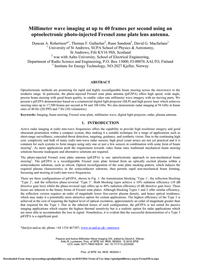
Millimeter wave imaging at up to 40 frames per second using an optoelectronic photo-injected Fresnel zone plate lens antenna. Duncan A. Robertson*1, Thomas F. Gallacher2, Rune Søndenå3, David G. Macfarlane1 1 University of St Andrews, SUPA School of Physics & Astronomy, St Andrews, Fife KY16 9SS, Scotland 2 was with Aalto University, School of Electrical Engineering, Department of Radio Science and Engineering, P.O. Box 13000, FI-00076 AALTO, Finland 3 Institute for Energy Technology, NO-2027 Kjeller, Norway ABSTRACT Optoelectronic methods are promising for rapid and highly reconfigurable beam steering across the microwave to the terahertz range. In particular, the photo-injected Fresnel zone plate antenna (piFZPA) offers high speed, wide angle, precise beam steering with good beam quality, to enable video rate millimeter wave imagery with no moving parts. We present a piFZPA demonstrator based on a commercial digital light projector (DLP) and high power laser which achieves steering rates up to 17,500 beams per second at 94 and 188 GHz. We also demonstrate radar imaging at 94 GHz at frame rates of 40 Hz (2D PPI) and 7 Hz (3D volumetric). Keywords: Imaging, beam steering, Fresnel zone plate, millimeter wave, digital light projector, radar, plasma antenna. 1. INTRODUCTION Active radar imaging at (sub) mm-wave frequencies offers the capability to provide high resolution imagery and good obscurant penetration within a compact system, thus making it a suitable technique for a range of applications such as short-range surveillance, concealed threat detection, targeting, guidance, and synthetic vision. Due to the continuing high cost, complexity and bulk of many (sub) mm-wave radar sensors, high pixel count arrays are not yet practical and it is common for such systems to form images using only one or just a few sensors in combination with some form of beam steering1. As more applications push the requirement towards video frame rates traditional mechanical beam steering solutions become inadequate and alternative solutions are required. The photo-injected Fresnel zone plate antenna (piFZPA) is one optoelectronic approach to non-mechanical beam steering2. The piFZPA is a reconfigurable Fresnel zone plate formed from an optically excited plasma within a semiconductor substrate, such as silicon. Optical reconfiguration of the zone plate masking pattern, which induces the required plasma characteristics in the semiconductor substrate, then permits rapid non-mechanical beam forming, focussing and steering at (sub) mm-wave frequencies. There are three configurations of piFZPA, shown in Fig. 1: the transmission blocking ‘Type 1’, the reflection blocking ‘Type 2’, and the reflection phase-reversal ‘Type 3’. Both blocking types achieve a 10% radiation efficiency (10 dB directive gain loss) whilst the phase-reversal type offers up to 40% radiation efficiency (4 dB directive gain loss). These losses are inherent to the binary forms of Fresnel zone plates. Although blocking Types 1 and 2 offer similar efficiency, the reflection version requires an order of magnitude lower free-carrier plasma density, and hence optical irradiance, which may make it a potentially more attractive option for certain applications. The highest efficiency of the Type 3 is achieved at the cost of requiring the highest level of optical excitation, approximately an order of magnitude greater than that required for the Type 1. Due to the inherent losses of each configuration, the piFZPA is not suited for passive imaging applications which require the highest thermal sensitivity but is a realistic option for radar applications which are more able to accommodate the loss in signal. Nonetheless, it is evident that the successful demonstration of a Type 3 piFZPA is a significant goal. *dar@st-and.ac.uk; phone +44 1334 467307; www.st-and.ac.uk/~mmwave Passive and Active Millimeter-Wave Imaging XIX, edited by David A. Wikner, Arttu R. Luukanen, Proc. of SPIE Vol. 9830, 983004 · © 2016 SPIE CCC code: 0277-786X/16/$18 · doi: 10.1117/12.2223026 Proc. of SPIE Vol. 9830 983004-1 Downloaded From: http://proceedings.spiedigitallibrary.org/ on 06/03/2016 Terms of Use: http://spiedigitallibrary.org/ss/TermsOfUse.aspx wave mm -wave (a) reflector (b) reflect r (c) Figure 1. Photo-injected Fresnel zone plate antenna (piFZPA) configurations: (a) transmission blocking Type 1, (b) reflection blocking type 2, and (c) reflection phase-reversal Type 3. SLM = spatial light modulator. The original work by Webb et. al. demonstrated the concept and potential of piFZPAs using systems configured at 20, 35 and 94 GHz based on silicon wafers with apertures up to 350 mm and illuminated by programmable arrays of near infrared (NIR) LEDs2, 3, 4, 5. In these configurations Webb achieved beam steering angles up to ±30° and rates up to 4,700 Hz3. In our previous work we demonstrated a Type 1 piFZPA at 94 GHz using a passivated silicon wafer illuminated with white light from a commercial data projector over an aperture of 100 mm. This achieved beam steering angles up to ±45° but rates were limited by the data acquisition software and losses were excessive due to non-optimum wafer thickness6, 7, 8, 9. This paper presents our recent work to address these shortcomings and outlines our development of a piFZPA demonstrator suitable for all three configurations. Our aims for this work have been to:1. Maximize efficiency by optimizing wafer thickness 2. Demonstrate high speed beam steering using digital light projector (DLP) projection technology 3. Demonstrate Type 2 (lower irradiance) and Type 3 (40% efficiency) piFZPAs 4. Demonstrate piFZPA operation frequencies above 94 GHz 5. Demonstrate radar imaging using high speed piFZPA beam steering Section 2 details the silicon processing and characterization needed to optimise wafer performance and accurately design the different types of piFZPA and section 3 describes the demonstrator hardware. The experimental results for the piFZPA are given in section 4 and the radar imaging experiments in section 5. 2. WAFER PROCESSING & CHARACTERIZATION High resistivity float zone silicon wafers of 6” diameter were used in this work and batches were thinned to the required thicknesses for transmission and reflection modes of operation by mechanical polishing and wet etching with HF. Each wafer was thinned to within 8-13 μm of the target value. The silicon wafers were passivated in order to reduce the surface recombination velocity (SRV) of the wafers, thus reducing the optical irradiance required to excite the require plasma densities – i.e. maximize the induced plasma density for a given optical irradiance. The chosen passivation method followed a standard process borrowed from the solar cell industry and involved removing surface defects and impurities via wet chemical etching, followed by a dry, high frequency plasma enhanced chemical vapor deposition (HFPECVD) of hydrogenated silicon nitride (SiNx:H) with a thickness of a few hundred nanometers. Type 2 and 3 configurations require an optically transparent mm-wave reflector to be deposited on the rear face of the wafer. Indium tin oxide (ITO) is a suitable material for this purpose as it can exhibit a high mm-wave reflectivity and a high optical transmission. ITO coatings with a surface resistance of 10 Ω/□ were deposited by a commercial vendor. Subsequent VNA measurements confirmed mm-wave reflectivity of the ITO layer to be >99% at 94 GHz. Following preparation of all the wafers, they were subjected to thorough and periodic characterization to establish their key material properties. This allowed us to monitor the temporal effects of the passivation process and to determine the stability of the wafer properties. Proc. of SPIE Vol. 9830 983004-2 Downloaded From: http://proceedings.spiedigitallibrary.org/ on 06/03/2016 Terms of Use: http://spiedigitallibrary.org/ss/TermsOfUse.aspx Initial characterizations of the minority free-carrier lifetimes were performed on each wafer batch using quasi steady state photoconductance (QSSPC) and microwave photoconductance decay (μPCD) instrumentation at the Institute for Energy Technology (IFE), Norway, and at Aalto University, Finland. QSSPC obtains a measure of the spatially averaged lifetime as a function of injection density using a white light arc lamp source. In contrast, μPCD uses a pulsed laser source and a CW microwave sensor (at ~10 GHz) to allow the lifetime to be mapped over the wafer surface with a spatial resolution of a few millimeters. All of the Type 1 wafers exhibited a long free-carrier lifetime, consistent with the high bulk resistivity and an effective passivation layer. Lifetimes ranged from 1680 μs to 2110 μs during the initial weeks following passivation. The Type 2/3 wafers without ITO coating also exhibited long lifetimes, in the region of 2540 μs. The ITO deposition causes a marked reduction in the lifetime by about a factor of 5-6 with measured lifetimes being in the range 400 to 500 μs. Critical aspects of the properties of the silicon wafers are understood by measuring their millimeter wave transmission and reflection as a function of frequency for different levels of optical excitation. Free-space transmission and reflection interferograms were obtained for the wafers over 75 – 100 and 140 – 220 GHz using a vector network analyzer (VNA) based quasi-optical (QO) bench9. The setup allows the wafers to be measured in the unilluminated state and with different levels of optical excitation from an external high power (white) light source (up to 600 mWcm-2). Fig. 2 shows example transmission interferograms for Type 1 wafers in the unilluminated and illuminated states. _o- loot = 0 mW/cm2 -o- w4 -Data -o- w6 -Data 30 I 100 opt = 200 mW/cm2 - o- lopi = 390 mW/cm2 -w4 - Model -w6 - Model 80 -o- -25 120 140 160 180 200 220 80 100 120 140 160 180 200 220 Frequency (GHz) Frequency (GHz) Figure 2. Example unilluminated Transmission interferograms with model fits for Type 1 wafers w4 & w6 (left) and Transmission versus frequency as a function of optical irradiance for Type 1 wafer w4 (right). The Type 1 wafers exhibited an unilluminated insertion loss of <0.25 dB at 94 GHz and <0.7 dB at 188 GHz with transmission maxima close to the chosen design frequencies. Such values are greater than would be expected for bulk high resistivity silicon which is well known to exhibit an extremely low dark state insertion loss. However, due to the passivated wafers becoming so sensitive to optical excitation (due to their lowered SRV) even the laboratory ambient light level was sufficient to cause a small increase in the imaginary part of the refractive index, thus raising the loss by a few tenths of a dB. In the optically excited cases, the insertion loss of a Type 1 wafer at 94/188 GHz changes from <0.25/0.7 dB in the unilluminated (ambient) state to 18 and 21 dB when illuminated with irradiances of 200 and 390 mWcm -2 respectively (i.e. it scales linearly). This change in transmission provides the contrast between the illuminated and unilluminated zones in a Type 1 blocking piFZPA. Unfortunately, an error in specifying the Type 2/3 wafers resulted in them being the wrong thickness for operation at 94 GHz where they exhibited a 6-10 dB loss due to the etalon effect of the ITO coating on the rear surface. However, insertion losses of <1 dB could be achieved by operating at frequencies of ~70, 125 or 185 GHz which are optimum for the actual wafer thickness but test equipment was not available at those frequencies in this instance. Ideally, the wafers could either be thinned further to the next resonantly matched thickness or new wafers purchased and accurately thinned. Unfortunately, neither option was possible in the project timeframe so measurements were performed at 94 GHz with the non-optimal thickness. Proc. of SPIE Vol. 9830 983004-3 Downloaded From: http://proceedings.spiedigitallibrary.org/ on 06/03/2016 Terms of Use: http://spiedigitallibrary.org/ss/TermsOfUse.aspx The optically excited behavior of a reflector-backed Type 2/3 wafer is more complicated than the Type 1 case due to the resonant etalon effect which it exploits. Fig. 3 shows the modeled reflectivity (amplitude and phase) of a Type 2/3 wafer as a function of plasma density. As the plasma density increases, the reflectivity amplitude drops as the silicon becomes absorbing, but the effect is enhanced over that of the Type 1 wafers by the etalon effect due to the rear reflector. In this example, the reflectivity amplitude drops to nearly zero at Δn ≈ 7 x 10 14 cm-3 which corresponds to the Type 2 configuration. At much higher plasma densities, the amplitude reflectivity rises back towards unity as a result of the semiconductor producing metallic-like behavior whilst the reflection phase flips by 180° from the dark state value. At Δn > 1016 cm-3, one approaches the Type 3 phase reversal configuration. ..... .. ..... ..... .. . . . ...... Type 3 ...... . ........ . . . . . .......... ... ... . " : ..... . . . ...... . ..... . . . . . -45 "." ..... - -135 Type 2 ..... . . . : ::: 221 1 017 1018 UL100 101 Figure 3. Modelled reflectivity (amplitude and phase) as a function of free carrier plasma density in a reflection mode Type 2/3 reflector-backed silicon wafer. 3. PIFZPA DEMONSTRATOR DESIGN Aside from a suitable silicon wafer, the piFZPA demonstrator requires a high power, high speed optical illumination system with which to project the zone masks onto the rear face of the silicon. Additionally, the millimeter wave beam must be coupled to the wafer, either from the same (rear) side as the optical excitation in a Type 1 configuration or from the opposite (front) side in Types 2 and 3. These aspects are described in the following section. At the heart of the projection system is a DLP evaluation board featuring a 1024 x 768 (XGA) pixel digital micro-mirror (DMD) chipset, capable of up to 30,000 frames per second, with onboard memory from which pre-stored binary zone mask files could be clocked out at high speed. A Class 4 fiber-coupled 75 W CW NIR diode laser operating at 808 nm with associated liquid-cooled chiller, OEM power supply module and armored optical fiber was used as the high power light source. Custom optics were required to couple the light from the laser fiber onto the DMD and then to project onto the silicon wafer. While incoherent sources (e.g. broadband arc lamps) could be used and may be more desirable for some applications, exploring alternative light sources was beyond the scope of the project and the laser was available. The requirements for the custom optics were to couple light from the output fiber of the NIR laser onto the DMD chipset with a uniform, top-hat, illumination and then project the zone plate mask pattern onto the silicon wafer with a diameter of ~140 mm. As the multi-mode fiber exhibited a flat top intensity distribution at the fiber end, one set of lenses was required to image the 600 μm fiber end onto the DMD to provide the necessary uniform input illumination, and a second set of lenses was needed to image the DMD onto the silicon wafer. The challenge was to achieve the relatively high levels of magnification (x17.5 from fiber to DMD and x13.3 from DMD to wafer) over a moderately short distance to yield a reasonably compact system. Off-the-shelf cage mount components and stock lenses were utilized to minimize cost and timescale but the resulting design has a longer throw than could be achieved with custom lenses. A custommade aluminum block to mount the cage optics onto the DMD at the required input and output angles (-24° input, 0° ‘on’ and +12° ‘off’ beams, all in the 45° plane) was designed, precision machined and optically blackened to reduce unwanted scattering. Additionally, as the DMD deflects approximately half the incident power (~ 20 W) from the ‘off’ pixels, a high power beam dump was designed and manufactured to terminate that beam. Proc. of SPIE Vol. 9830 983004-4 Downloaded From: http://proceedings.spiedigitallibrary.org/ on 06/03/2016 Terms of Use: http://spiedigitallibrary.org/ss/TermsOfUse.aspx For Type 1 configurations in which the mm-wave beam and optical excitation are both incident from the rear side of the wafer, an ITO-on-polymer beamsplitter was chosen to couple the two beams (15 Ω/□ ITO on 175 μm thick polyester film). The optical excitation passed straight through the beamsplitter with a transmission of 78% whilst the mm-wave beam was incident from the side and reflected off the beam splitter with >99% reflectivity. For Type 2/3 configurations, in which the optical excitation is incident on the rear wafer surface whilst the mm-wave beam is incident on the front wafer surface, a mm-wave prime fed arrangement was selected (and the ITO-on-polymer beamsplitter removed). Finally the entire piFZPA assembly was mounted on 600 x 600 mm optical breadboard and surrounded by an interlocked light-tight enclosure to achieve a laser classification for the assembly of Class 1, meaning that it could be used outside of a laser lab for piFZPA testing – Fig. 4. Laser Beam dump Cage mount optics DMD Feed Fiber end Receiver ITO beam splitter Data Acquisition Silicon wafer Figure 4. Plan view of piFZPA assembly in Type 1 configuration for one-way (receive) antenna pattern measurements. Final optical testing of the piFZPA illumination system yielded the following results. With the laser running at the maximum available current of 55 A, the optical power out of the fiber was 67 W. The total power measured at the silicon plane was 37.3 W, with a maximum power density of 240 mWcm-2 over an area of 154 cm2 (140 mm diameter). Thus the entire optical assembly was measured to have an optical transmission of 56%. Accounting for the efficiency of the DMD which is quoted as 60%, the custom optics thus achieved a transmission of 93% which is in very good agreement with the ZEMAX prediction of 94%. No problems were noticed with regard to power handling and thermal management for any of the components. Beam profiles (1D) of the NIR illumination were measured at the silicon plane and showed a good uniformity in power density across the majority of the desired aperture – Fig. 5. The output distribution at the silicon plane was found to be quite flat, varying by only ±10% over a lateral extent of 120 mm. The presence of the ITO-on-polymer beamsplitter (for Type 1), which has a transmission of 79% at 808 nm, reduced the power density to 200 mWcm -2 in a vertical strip in the middle of the mask pattern. Proc. of SPIE Vol. 9830 983004-5 Downloaded From: http://proceedings.spiedigitallibrary.org/ on 06/03/2016 Terms of Use: http://spiedigitallibrary.org/ss/TermsOfUse.aspx 260 240 220 G 200 E 3 180 E 16o -No ITO Ñ 140 pp [mW/un2[ 120 No ITO [mW/un2[ 100 0 a 80 -80 -70 -60 -50 -40 -30 -20 -10 0 10 30 40 50 60 70 20 80 X position [mm] Figure 5. Photo of maximum power (37 W) NIR beam on paper target at plane of silicon wafer (left) and corresponding beam scan of optical power density across the silicon wafer plane, with and without ITO beamsplitter (right). 4. PIFZPA RESULTS The far-field antenna patterns of the piFZPA in different configurations were measured in receive for both on- and offaxis. A remote Gunn oscillator with 20 dBi feedhorn was used as the far-field source and the piFZPA acted as receive antenna fitted with a heterodyne downconverter. The received IF signal was amplified and measured using a detector diode as a function of beam steering angle. Measurements were made in a Type 1 configuration at 94 GHz and 188 GHz and in a Type 2 configuration at 94 GHz with reduced efficiency as noted above. Unfortunately the maximum power density achievable with the optical projection system was insufficient to achieve a successful Type 3 piFZPA at 140 mm diameter. To evaluate beam steering speed, the remote source was imaged with the piFZPA (typically ±20° in azimuth, ±10° in elevation, 0.25° increments) to yield 2D antenna patterns at different DMD frame rates from 500 fps to the maximum achievable with the test software of ~17,500 fps. One DMD frame corresponds to one mm-wave beam. Typical results are shown in Fig. 6 (left) which shows the excellent 2D symmetry obtained at 500 fps and how the 1D pattern changes as the frame rate is increased. As the frame rate increases beyond that consistent with the wafer lifetime, it is clear the peak gain reduces, the mainlobe width increases, the main lobe squints, and the peak sidelobe level degrades. Nonetheless, beam steering is achieved at 17,000 fps and acceptable performance is maintained up to several kHz depending on wafer lifetime. Similar results were obtained at 188 GHz which demonstrated the decreased beamwidth compared to 94 GHz for the same aperture diameter - Fig. 6 (right). 500 fps -20 -94 GHz -188 GHz -25 m -0 20 -10 0 10 Azimuth (deg) `m ó -30 a .A.IAhry, -35 -20 -15 -10 -5 0 5 10 15 20 azimuth (deg) 20 -20 -10 0 azimuth (deg) 10 Figure 6. Azimuth cuts through 2D antenna patterns as a function of frame rate (500 to 17,000 fps) for a Type 1 piFZPA at 94 GHz with 2D pattern at 500 fps inset (left) and comparison of azimuth cuts at 94 and 188 GHz. Proc. of SPIE Vol. 9830 983004-6 Downloaded From: http://proceedings.spiedigitallibrary.org/ on 06/03/2016 Terms of Use: http://spiedigitallibrary.org/ss/TermsOfUse.aspx 20 For the Type 1 configuration, the ambient loss was low for all wafers (~0.25 to 0.5 dB at 94 GHz) and the wafer thickness was very close to optimal. To achieve full blocking with 40 dB attenuation requires a carrier density of >10 16 cm-3. However, as shown in Fig. 2 only 18 dB of attenuation was achievable with ~200-240 mWcm-2 irradiance. This introduced a reduction in the piFZPA gain of ~3 dB (i.e. a drop of 50% in efficiency). Thus the net antenna efficiency achieved for the Type 1 configuration was 4.5 to 5% (i.e. half the maximum achievable). This was verified with the link gain budget in the antenna experiments. Nonetheless, this represents a 5x improvement over our previous work for the efficiency of a Type 1 piFZPA. The Type 2 configuration offers 10% efficiency at much lower irradiance than Type 1 by exploiting the sensitivity of the silicon-ITO etalon to the complex permittivity of silicon. To get full blocking (>40 dB attenuation) requires a carrier density of only ~7 x 1014 cm-3 which was easily achieved with an irradiance of just ~15 mWcm-2 for these wafers (just 2.3 W total optical power). However, the combination of the Type 2 wafers being the wrong thickness and their resonant sensitivity to the background ambient light meant the loss in the wafers increased by e.g. ~5-6 dB for wafer rx3. Thus the net antenna efficiency achieved for the Type 2 configuration was only 2 to 3%. These results do, however, confirm the key advantage of the Type 2 piFZPA, namely operation at much lower optical irradiance, which in this case was a factor of ~13 lower than for our Type 1 piFZPA. To achieve a 40% efficient Type 3 piFZPA will require selection of wafers with the correct thickness and either a projection system with much higher power and/or a reduction in the diameter of the piFZPA to reach the irradiance required for metallic-like behavior in silicon (~600 mWcm-2). Demonstrating a Type 3 piFZPA remains one of our objectives for future work. 5. RADAR IMAGING One of the primary motivations for pursuing the piFZPA technology is its use in active mm-wave radar imaging systems hence we have combined the piFZPA setup outlined above with our existing SAFIRE 94 GHz FMCW close-range imaging radar10. SAFIRE uses a circulator-based single antenna front-end and thus was fairly easily modified to be used with the piFZPA. The transceiver was connected to the piFZPA feed and the DMD frame trigger signal routed to SAFIRE’s control electronics, triggering the frequency chirps and data acquisition. A substantial modification of SAFIRE’s processing and display software was necessary in order to run the piFZPA in high speed 3D and 2D radar imaging modes. In particular, the modified software had to leverage the power of OpenGL graphics routines to allow the radar control computer to capture and display the images received by the piFZPA at such high rates. The piFZPA was used in Type 1 and Type 2 configurations for the radar imaging experiments. For maximum radar imaging resolution, SAFIRE was operated at its highest chirp bandwidth of 2 GHz, yielding a range resolution of 7.5 cm, in a sweep time of ≥ 64 μs. Typically, 1024 range bins were processed but the displayed maximum instrumented range was limited to 25 m (corresponding to the back wall of the room). The one-way beamwidth in all cases was ~2.5° (140 mm aperture). Two radar imaging configurations were performed, as detailed below: (i) azimuthal scanning to form wide angle 2D PPI movies, and (ii) az-el scanning of moderate fields-of-view (FOV) to form 3D movies. The piFZPA-radar setup utilized an F/1.93 Type 1 configuration and an F/1.23 Type 2 configuration, operating at their respective efficiencies discussed above. In the 2D PPI mode, the piFZPA was raster-scanned in azimuth whilst the radar recorded range profiles for every angular position. Fig. 7 shows a snapshot from a 2D PPI movie and video recording in which the beam was swept over 40° in 0.1° increments (i.e. 401 azimuth beams) at ~8,000 beams per second, resulting in a PPI frame rate of 20 Hz. Due to the low efficiency of the Type 1 and 2 configurations, +20 dBsm trihedrals were used as bright targets and two can be clearly seen in the PPI plot. The highest 2D PPI radar imaging frame rate achieved in this configuration was 40 Hz. The very high PPI frame rates possible with the piFZPA were demonstrated by having the volunteers sprint up and down the FOV whilst holding the trihedrals – the piFZPA-based radar imager had no difficulty smoothly following this fast motion. Proc. of SPIE Vol. 9830 983004-7 Downloaded From: http://proceedings.spiedigitallibrary.org/ on 06/03/2016 Terms of Use: http://spiedigitallibrary.org/ss/TermsOfUse.aspx Figure 7. Snapshot of radar data and video capture for a 40° wide 2D PPI recorded at 20 Hz frame rate. The volunteers are holding trihedrals to provide bright targets and are running to demonstrate the high frame rate. In the 3D radar movie mode, the piFZPA was raster-scanned in azimuth and elevation whilst the radar recorded range profiles for every angular position (e.g. each radar image frame comprised 41 x 21 x 1024 samples). Fig. 8 shows a snapshot from a 3D radar movie and video in which the beam was raster-scanned over 20° x 10° in 0.5° increments (i.e. 41 azimuth x 21 elevation beams) at ~3,000 beams per second resulting in a 3D radar imaging frame rate of 3.5 Hz. The 3D data set is presented as a 2D projection of the maximum power values in each line of sight. In this configuration, 3D radar imaging frame rates up to 7 Hz were achieved. The high frame rate of the piFZPA-based 3D radar imager copes well with the dynamic nature of moving targets with minimal jitter or lag. [1 Figure 8. Snapshot of 3D radar data and video capture for a 20° x 10° field of view recorded at 3.5 Hz frame rate in which the volunteer is waving a trihedral to demonstrate the dynamic response (top). Single frame from this data set presented as front view projection of maximum power (lower left) and plan/PPI view (lower right). Proc. of SPIE Vol. 9830 983004-8 Downloaded From: http://proceedings.spiedigitallibrary.org/ on 06/03/2016 Terms of Use: http://spiedigitallibrary.org/ss/TermsOfUse.aspx Clearly the performance of the piFZPA degrades gradually with increasing beam steering rate (Fig. 6) so it is a matter of choice how fast a given setup can be steered whilst still achieving an acceptable level of performance. Primarily the speed response of a piFZPA is determined by the free carrier lifetime of the silicon which for the wafers used here (lifetimes in the ~0.5 to 2 ms range) corresponds to beam steering rates in the low kHz. Higher steering rates would be possible with less reduction in performance for wafers with shorter lifetimes but this requires higher irradiance levels. Another factor which may constrain the achievable radar imaging rate is the requirement to use very short chirps and the high data processing rate. In the case of SAFIRE, which uses a voltage controlled oscillator to generate the chirps, very short chirp times lead to degradation of the radar’s point response. However, other chirp generation methods such as direct digital synthesis (DDS) can overcome such problems. At radar imaging frame rates of e.g. 8,000 – 10,000 fps the input data rate, processing load (e.g. FFT processing of FMCW chirps) and data display rate become substantial which places demands on the controlling computer. However, with the trend of increasing computer processing power and the availability of GPU and FPGA technology it is unlikely that this would be a significant barrier to successful deployment of a future piFZPA-based radar imager. 6. DISCUSSION & CONCLUSIONS We have summarized the design and development of an advanced piFZPA demonstrator which combines carefully processed silicon wafers with a high power diode laser and a commercial DLP spatial light modulator for rapid zone plate mask reconfiguration to achieve high speed mm-wave beam steering using no moving parts. The demonstrator supports all three piFZPA configuration options, Types 1, 2 & 3 and the advantages and disadvantages of each type have been briefly summarized. Using newly sourced and processed silicon wafers we have reduced the mm-wave losses imposed by the substrate resulting in performance improvements compared to our previous work of up to a factor of 5 in certain configurations, whilst simultaneously increasing the realized aperture size by 40%. We have demonstrated the performance of a Type 1 piFZPA, with a 140 mm diameter aperture, at 94 and 188 GHz. The beam forming and scanning performance of this setup have been evaluated using full 2-D antenna pattern and off-axis measurements, up to +/- 45 from boresight. We believe that 188 GHz is the highest reported frequency of operation for a piFZPA. We have also observed and briefly discussed the good agreement between measured on-axis beam performance and the simulated results utilising custom piFZPA models. The realized radiation efficiency of this setup was measured to be between 4 – 5 % due to non-perfect matching of the wafer thickness to the operation frequency. This still represents a x5 improvement over our prior work. A similar set of measurements and characterisations were performed for a Type 2 piFZPA at 94 GHz, which aptly demonstrates the advantages of lower optical irradiance requirements: 15 mWcm-2 for Type 2 versus 200 mWcm-2 for Type 1. However, due to an unforeseen error with the wafer thickness, this configuration exhibited excess loss and the measured radiation efficiency was approximately 3 % rather than the maximum possible value of 10%. Due to the design choices of our piFZPA demonstrator setup (aperture size, illuminating source, wafer characteristics) the system did not have sufficient irradiance at the silicon plane to achieve a Type 3 piFZPA configuration. We aim to modify the demonstrator to reduce the illuminated aperture diameter to achieve sufficient irradiance for successful demonstration of a Type 3 piFZPA. In all configurations that were realized we have demonstrated rapid beam steering with beam rates of up to 17,500 beams per second. We believe that these rates are the highest reported for any beam steering antenna at these frequencies. Utilizing these beam rates, we have successfully demonstrated active radar imaging at 94 GHz using a close-range FMCW radar sensor and have achieved results from both 2D PPI images at up to 40 Hz and 3D volumetric imagery at up to 7 Hz. These results demonstrate a 3-order-of-magnitude increase in beam steering rate over our original projectorbased experiments. Whilst there is still work to be done to further improve the efficiency, the flexible and highly dynamic capability of the piFZPA for radar imaging has been clearly demonstrated and this technology is a potential candidate for a wide range of active imaging applications. Proc. of SPIE Vol. 9830 983004-9 Downloaded From: http://proceedings.spiedigitallibrary.org/ on 06/03/2016 Terms of Use: http://spiedigitallibrary.org/ss/TermsOfUse.aspx 7. ACKNOWLEDGEMENTS The authors thank Dr S. E. Foss, Institute for Energy Technology, P.O. Box, NO-2027 Kjeller, Norway, for access to the silicon wafer processing facilities. This work was partially funded by both the UK Engineering and Physical Sciences Research Council (EPSRC) and the Department of the Army, U.S. Army Research Office under Contract No. W911NF12-1-0535 / R&D 1528-EE-01. REFERENCES [1] R. Appleby, and B. Wallace, “Standoff detection of weapons and contraband in the 100GHz to 1THz region," IEEE Antennas and Propagation Magazine, 55(11), 2944 – 2955 (2007). [2] G. W. Webb, and L. H. Pinck, “Light-controlled MMW beam scanner,” SBMO International Microwave Conference/Brazil, 2, 417 – 422 (1993). [3] G. W. Webb, S. C. Rose, M. S. Sanchez, and J. M. Osterwalder, “Experiments on an optically controlled 2-d scanning antenna," Antenna Applications Symposium, , 99 – 113 (1998). [4] G. W. Webb, W. Vernon, M. S. Sanchez, S. C. Rose, and S. Angello, “Optically controlled millimeter wave antenna,” International Topical Meeting on Microwave Photonics, , 275 - 278 (1999). [5] G. W. Webb, S. Angello, W. Vernon, M. S. Sanchez, and S. C. Rose, “Novel photonically controlled antenna for MMW communication," International Topical Meeting on Microwave Photonics, , 97 - 100 (2000). [6] T.F. Gallacher, R. Sondena, D.A. Robertson, and G.M. Smith, “Optical Modulation of Millimeter-Wave Beams Using a Semiconductor Substrate,” IEEE Trans. Microwave Theory Tech., 60(7), 2301 – 2309 (2012) [7] T.F. Gallacher, D.A. Robertson, and G. M. Smith, “The Photo-Injected Fresnel Zone Plate Antenna: Optoelectronic Beam Steering at mm-Wave Frequencies,” IEEE Trans. Antennas Propag., 61(4), 1688 – 1696 (2013) [8] T. F. Gallacher, R. Sondena, D. A. Robertson and G. M. Smith, "Off-Axis Measurements on a mm-Wave Optically Controlled Lens Antenna," IEEE Antennas and Wireless Propagation Letters, 12 , 1520 - 1522 (2013) [9] T.F. Gallacher, “Optoelectronic Modulation of mm-Wave Beams Using a Photo-Injected Semiconductor Substrate,” PhD Thesis University of St Andrews, , (2012) [10] D.G. Macfarlane, and D.A. Robertson, “SAFIRE: A real time close range millimetre wave exhibition radar,” 35th Int. Conf. Infrared Millimeter and Terahertz Waves, 1, , 1 – 2 (2010) Proc. of SPIE Vol. 9830 983004-10 Downloaded From: http://proceedings.spiedigitallibrary.org/ on 06/03/2016 Terms of Use: http://spiedigitallibrary.org/ss/TermsOfUse.aspx
