Solid-State Electronics 47 (2003) 2081–2084
www.elsevier.com/locate/sse
Quasi-enhancement mode AlGaN/GaN HEMTs
on sapphire substrate
Jaesun Lee a, Dongmin Liu a, Zhaojun Lin a, Wu Lu
George R. Brandes b
a
a,*
, Jeffrey S. Flynn b,
Department of Electrical Engineering, The Ohio State University, 205 Dreese Labs, 2015 Neil Avenue,
Columbus, OH 43210, USA
b
ATMI, Danbury, CT 06810, USA
Received 10 May 2003; accepted 22 May 2003
Abstract
In this study, quasi-enhancement mode AlGaN/GaN HEMT devices with the gate length of 1-lm are fabricated
using a conventional method (i.e. without gate-recessing process) and the direct current and radio frequency characteristics of these devices are investigated. The threshold voltages are in the range of )0.3 to )0.5 V. The devices exhibit a
maximum drain current of 280 mA/mm at a gate bias of 2 V. The pinch off voltage is about )1.0 V. At the gate bias of
1.5 V and the drain bias of 6 V, the devices exhibit an extrinsic transconductance of 140 mS/mm, a unity current gain
cutoff frequency (fT ) of 4.3 GHz, and a maximum oscillation frequency (fMAX ) of 13.3 GHz, respectively.
Ó 2003 Elsevier Ltd. All rights reserved.
PACS: 85.30.T; 81.05.D
1. Introduction
There have been extensive efforts to develop GaN and
the related alloys for electronic device applications.
GaN-based HEMT studies have been concentrated on
the development of microwave power devices. Up to
now, efforts have been focused on the depletion mode
AlGaN HEMTs devices with pinch-off voltages typically
in the range of )4 to )8 V, which have demonstrated
excellent microwave power performances [1,2]. Enhancement-mode GaN-based HEMTs are of interests
because they can be integrated with the depletion-mode
devices to form complementary circuits. However, high
polarization charge density at the interface between
AlGaN and GaN limits the fabrication of enhancement
mode HEMT devices. An enhancement mode AlGaN/
GaN HEMT requires theoretically about several na-
*
Corresponding author. Tel.: +1-614-292-3462; fax: +1-614292-7596.
E-mail address: lu@ee.eng.ohio-state.edu (W. Lu).
nometer AlGaN thickness and about 20% of Al mole
concentration. Khan et al. [6] reported an enhancement
mode AlGaN/GaN HFET using a low pressure
MOCVD system. In this enhancement device, a much
thinner AlGaN layer with the thickness of 10 nm compared to that of depletion mode devices was used. With
the use of a thin barrier layer and the adjustment of the
barrier layer doping, the threshold voltage of 0.05 V was
achieved. However, the dc transconductance was only
23 mS/mm for a device with 1 lm gate length and 5 lm
drain to source separation. To improve device performance, a few attempts to fabricate the enhancement
mode devices have been performed. Using a gaterecessing process, the threshold voltage can be controlled by the etching depth [1,4,5]. Moon et al. [3]
reported the fabrication of the enhancement mode AlGaN/GaN HEMTs with 0.2 lm gate length and 200 lm
gate width using a gate recessing process. These devices
exhibited a maximum drain current density of 100 mA/
mm, a peak transconductance (gm ) of 85 mS/mm, an
unity current gain cut-off frequency (fT ) of 24 GHz, and
a maximum oscillation frequency (fMAX ) of 45 GHz.
0038-1101/$ - see front matter Ó 2003 Elsevier Ltd. All rights reserved.
doi:10.1016/S0038-1101(03)00245-4
2082
J. Lee et al. / Solid-State Electronics 47 (2003) 2081–2084
These performances are limited due to large access resistance. Hu et al. [7] fabricated an enhancement mode
AlGaN/GaN HEMTs with a gate length of 10 lm and a
gate width of 150 lm by using selectively grown pn
junction gate. This selective growth technique allowed
both enhancement and depletion mode to be fabricated
on the same wafer, thus, provided the possibility for the
low consumption GaN-based logical integrated circuits.
However, this enhancement device still showed very
small gm value of 10 mS/mm and the maximum saturation current of 40 mA/mm at a gate bias of 4 V.
In this study, quasi-enhancement mode AlGaN/GaN
HEMT devices with 1-lm gate length are fabricated
with no gate-recessing and DC and RF characteristics of
these devices are investigated.
2. Device layer structure and fabrication
The device cross section is shown in Fig. 1. The epilayer of AlGaN/GaN HEMT structure shown in Fig. 1
was grown by metal-organic chemical vapor deposition
(MOCVD) on a (0 0 0 1) sapphire substrate. The epilayer
consists of 40 nm AlN nucleation layer, 3 lm of undoped GaN, and 20 nm undoped Al0:25 Ga0:75 N. Hall
measurements indicated that the layer had a twodimensional sheet carrier density of 9 1012 cm 2 and an
electron mobility of 1100 cm2 /v s at room temperature,
respectively. Device isolation was performed by mesa
dry etching using an inductively coupled plasma reactive
ion etching system in a chlorine-based plasma and using
photoresist as an etch mask. Ti/Al/Mo/Au drain–source
ohmic contacts were deposited using electron beam
evaporation and annealed at 900 °C for 30 s in a rapid
thermal annealing system. The ohmic contact resistivity
was determined typically to be 4 10 8 X cm 2 using
transfer length measurement patterns, hence, excellent source access resistance was achieved. Ni/Au metallization was used for Schottky gate contacts with a
gate length of 1 lm. The devices have a gate width of
100 lm and the source to drain spacing of 3 lm. All
patterning were performed using optical contact lithography.
3. Results and discussion
The measurements of DC and microwave characteristics were performed using Agilent 4156C semiconductor parameter analyzer and Agilent 8510C network
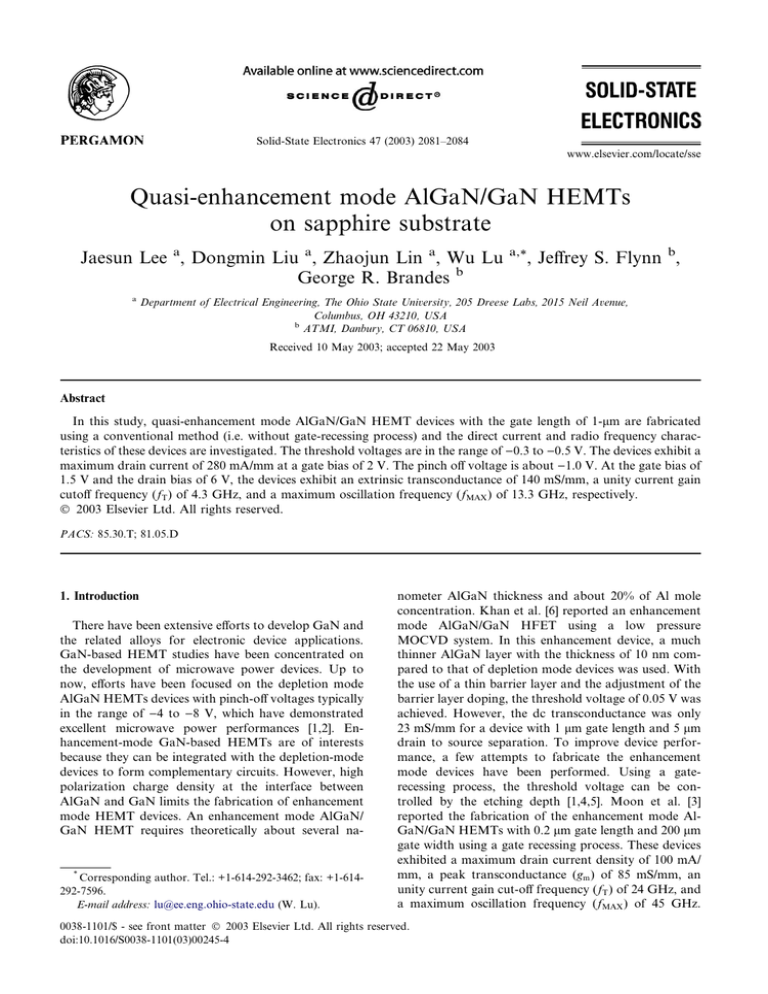
analyzer. Fig. 2 shows the typical drain current–voltage
characteristics of the T -configuration HEMT devices
with 1-lm gate length and 100-lm gate width. The gate
bias is in the range of )1.5 to 2 V with the step of 0.5 V.
The maximum drain current at a gate bias of 2 V is 280
mA/mm and the drain current at a gate bias of 0 V (Vdss )
is 59 mA/mm. The knee voltage is about 1.5 V. These
devices have the typical pinch-off voltage of about )1.0
V. Generally, depletion mode AlGaN/GaN HEMT devices have very high pinch-off voltages, typically in the
range of )4 to )8 V. Some of the devices clearly show
kinks in the drain characteristics. This effect is attributed
to the hot electron injection and trapping in the buffer
layer [5]. The drain current–voltage characteristics at the
higher bias voltages exhibit negative differential resistance characteristic due to the self-heating effect and the
poor thermal conductivity of the sapphire substrates [8].
The maximum drain current value of our devices is
larger than those of reported enhancement mode HEMT
devices fabricated with other techniques. As mentioned
earlier, the maximum drain current of the enhancement
300
G
Al0.25Ga0.75N
20 nm
GaN
2V
250
D
Drain Current (mA/mm)
S
1.5 V
200
1.0 V
150
0.5 V
100
0V
50
0
0
Sapphire Substrate
Fig. 1. AlGaN/GaN HEMT layer structure.
3
6
9
12
- 0.5 V
-1.0 V
15
Drain Voltage (V)
Fig. 2. DC I–V characteristics of a 1 lm AlGaN/GaN HEMT
with a gate width of 100 lm. The gate was biased from )1.5 to
2 V.
J. Lee et al. / Solid-State Electronics 47 (2003) 2081–2084
Gate Current (mA/mm)
250
100
200
150
100
50
50
Transconductance (mS/mm)
150
300
Vth
0
0
-2
-1
0
1
2
Gate to Source Voltage (V)
Fig. 3. DC transfer characteristics of an AlGaN/GaN with a
gate width of 100 lm and a gate length of 1 lm. The threshold
voltage of the device is )0.3 V.
20
20
15
15
MSG/MAG
10
10
h21
5
5
0
0
1
tion gate was only 10 mS/mm, respectively. From the
gate-bias intercept of the extrapolation of drain current
curve at the peak gm position in the transfer characteristics, the threshold voltages are determined in the range
of )0.3 to )0.5 V depending on drain bias voltages.
These threshold voltages are much smaller than those
of the typical values of conventional AlGaN/GaN
HEMTs, which are typically in the range of )5 to )8 V.
The small signal RF measurements of 1-lm enhancement mode AlGaN/GaN HEMTs were performed in the
range of 1–50 GHz. Fig. 4 shows the plots of current
gain and maximum stable power gain (MSG) and
maximum available gain (MAG) versus frequency. The
devices with a gate length of 1 lm exhibited an fT of 4.3
GHz and an fMAX of 13.3 GHz at a gate bias of 1.5 V
and a drain bias of 6 V. According to our knowledge,
these are the highest reported values for GaN-based
enhancement devices with the same gate length. With
further optimization of device structures, GaN-based
enhancement mode HEMTs with better device performances are expected in the near future.
4. Conclusions
Quasi-enhancement mode AlGaN/GaN HEMT devices with 1-lm gate length are fabricated without using
gate-recessing process or selectively grown pn junction
gate technique. These quasi-enhancement mode devices
exhibit the threshold voltage of as low as )0.3 V, a gm of
140 mS/mm, an fT of 4.3 GHz, and an fMAX of 13.3
GHz, respectively. Further improvement of enhancement-mode GaN-based HEMT devices is desired for
applications of complementary integrated circuits.
Acknowledgements
MSG/MAG (dB)
Current Gain (dB)
mode devices with gate recessing was 100 mA/mm and
that of devices with selectively grown pn junction gate
was only 40 mA/mm even at the gate bias of 4 V.
The typical DC transfer characteristics of the devices
are shown in Fig. 3. A maximum extrinsic transconductance (gm ) of 140 mS/mm is obtained at a gate
voltage of 1.4 V and at a drain bias voltage of 3.5 V.
This peak gm value is much lager than that of devices
fabricated by gate-recessing or selectively grown pn
junction gate technologies. The peak gm of the enhancement mode devices with gate recessing was 85 mS/
mm and that of devices with selectively grown pn junc-
2083
10
Frequency (GHz)
Fig. 4. Current gain and maximum stable power gain versus
frequency of an AlGan/GaN with a gate width of 100 lm and
a gate length of 1 lm. The gate bias is 1.5 V and a drain bias is
6 V.
The authors thank Dr. P.R. Berger for assistance on
RTP annealing and Dr. V. Kumar for technical assistance on mesa etching. The work at OSU was partially
supported by National Science Foundation DMR0216892.
References
[1] Kumar V, Lu W, Khan FA, Schwindt R, Kuliev A, Yang J,
et al. IEDM Technical Digest, Washington DC; 2001.
[2] Kumar V, Lu W, Khan FA, Schwindt R, Kuliev A, Yang J,
et al. Electron Lett 2002;38:252.
[3] Khan MA, Chen Q, Sun CJ, Yang JW, Shur MS, Park H.
Appl Phys Lett 1996;68:514.
2084
J. Lee et al. / Solid-State Electronics 47 (2003) 2081–2084
[4] Binari SC, Ikossi K, Roussos JA, Kruppa W, Park D,
Dietrich HB, et al. IEEE Trans Electron Dev 2001;48:
465.
[5] Moon JS, Wong D, Hussain T, Micovic M, Deelman P, Hu
M, et al. The 60th Device Research Conference. Santa
Babara, California; 2002. p. 23–5.
[6] Moon JS et al. Proceedings of International Symposium of
Compound Semiconductor. Komaba, Japan; 2001.
[7] Hu X, Simin G, Yang J, Khan MA, Gaska R, Shur MS.
Electron Lett 2000;36:753.
[8] Ping AT, Chen Q, Yang JW, Khan MA, Adesida I. IEEE
Electron Dev Lett 1998;19:54.


