An Intuitive Approach To Understanding Current
Feedback Amplifiers
®
October 11, 2004
Application Note
AN9787.1
Introduction
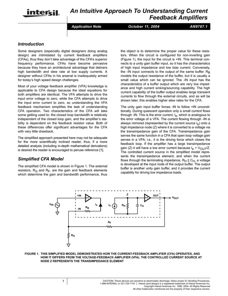
the object is to determine the proper value for these resistors. When the circuit is configured for non-inverting gain
(Figure 1), the input for the circuit is +IN. This terminal connects to a unity gain buffer input, so it has the characteristics
of high input impedance and low bias current. Conversely,
the -IN input connects to the output of the same buffer. RB
models the output resistance of the buffer, but it is usually a
small value which can be ignored. The -IN input has the
characteristics of a buffer output which are very low impedance and high current sinking/sourcing capability. The high
current capability of the buffer output enables large transient
currents to flow through the external circuits, and as will be
shown later, this enables higher slew rates for the CFA.
Some designers (especially digital designers doing analog
design) are intimidated by current feedback amplifiers
(CFAs), thus they don’t take advantage of the CFA’s superior
frequency performance. CFAs have become pervasive
because they have an architectural advantage that delivers
high bandwidth and slew rate at low supply currents. A
designer without CFAs in his arsenal is inadequately armed
for today’s high speed design challenges.
Most of your voltage feedback amplifier (VFA) knowledge is
applicable to CFA design because the ideal equations for
both amplifiers are identical. The VFA attempts to drive the
input error voltage to zero, while the CFA attempts to drive
the input error current to zero, so understanding the VFA
feedback mechanism simplifies the task of understanding
CFA operation. Two characteristics of the CFA will take
some getting used to: the closed loop bandwidth is relatively
independent of the closed loop gain, and the amplifier’s stability is dependent on the feedback resistor value. Both of
these differences offer significant advantages for the CFA
with very little drawback.
The unity gain input buffer forces -IN to follow +IN unconditionally. During quiescent operation only a small current flows
through -IN. This is the error current, Ie, which is analogous to
the error voltage of a VFA. The current flowing through -IN is
always mirrored (represented by the current source Ie) onto a
high impedance node (Z) where it is converted to a voltage via
the transimpedance gain of the CFA. Transimpedance gain
serves the same function in a CFA that open loop voltage gain
serves in a VFA; i.e., it is the driving force which closes the
feedback loop. If the amplifier has a large transimpedance
gain (Z) it will have a low error current because Ie = VOUT/Z.
The controlled current source in the simplified model represents the transimpedance element, and when the current
flows through the terminating impedance, RH || CH, a voltage
is developed at the input node of the output buffer. The output
buffer is another unity gain buffer, and it provides the current
capability for driving low impedance loads.
The simplified approach presented here may not be adequate
for the more scientifically inclined reader, thus, if a more
detailed analysis (including in-depth mathematical derivations)
is desired the reader is encouraged to peruse reference [1].
Simplified CFA Model
The simplified CFA model is shown in Figure 1. The external
resistors, RG and RF, are the gain and feedback elements
which determine the gain and bandwidth performance, thus
Z
+IN
+1
+1
VIN
-IN
RB
Ie
Ie
RH
OUT
VOUT
CH
RF
RG
FIGURE 1. THIS SIMPLIFIED MODEL DEMONSTRATES HOW THE CURRENT-FEEDBACK AMPLIFIER (CFA) OPERATES, AND
HOW IT DIFFERS FROM THE VOLTAGE-FEEDBACK AMPLIFIER (VFA). THE CONTROLLED CURRENT SOURCE AT
NODE Z REPRESENTS THE TRANSIMPEDANCE ELEMENT
1
CAUTION: These devices are sensitive to electrostatic discharge; follow proper IC Handling Procedures.
1-888-INTERSIL or 321-724-7143 | Intersil (and design) is a registered trademark of Intersil Americas Inc.
Copyright Intersil Americas Inc. 1998, 2004. All Rights Reserved
All other trademarks mentioned are the property of their respective owners.
Application Note 9787
For example, consider a voltage follower (RG = infinity)
where at t = 0 V+IN = VOUT = 0. If at t = 0+ a unit step voltage is applied to the input, then at t = 0+ V+IN = V-IN = 1V,
and VOUT -VIN = -1V, thus Ie = -1V/RF. Notice that the slew
current, Ie, is dependent on the magnitude of the output voltage change and RF. This error current is sourced by the
input buffer, so an equal current is mirrored onto node Z,
causing the voltage to rise, and consequently the output voltage increases. The feedback loop keeps VOUT rising until
the error current is driven to the minimum value, and at this
point V+IN = VOUT within the error tolerance.
Analyze CFA Amplifiers Just Like VFA
Amplifiers
The same four “ideal op amp” assumptions employed to
derive the VFA closed loop gain equations are used to derive
the ideal CFA closed loop gain equations. By definition,
V-IN = V+IN because the element separating the two inputs
is a well designed unity gain buffer. The non-inverting input
current is low enough to be neglected (+IN = 0) because this
current is a buffer input current. The inverting input current
equals zero (-IN = 0) because the feedback loop drives the
error current to zero. As long as the transimpedance gain is
large the -IN current is negligible. It is prudent to note that
the two input currents are totally uncorrelated, thus the common VFA technique of canceling input current errors by balancing the impedance seen at the positive and negative
inputs is not recommended for CFAs. The transimpedance
gain is extremely high, which enables the feedback loop to
function properly just like high open loop gain does in a VFA.
The feedback network is constructed the same for the CFA
and VFA; a feedback resistor (RF) is connected from the op
amp output to the inverting input, and a gain setting resistor
(RG) is connected from the inverting input to ground in both
cases. Because the feedback network is the same for the
CFA and VFA, and because the ideal op amp assumptions
are valid for both types, it is obvious that the VFA ideal
closed loop gain equation must hold for the CFA.
The non-inverting gain formula, Equation 1, is based on
these assumptions; the voltage across RG is VIN because
-IN tracks +IN, so the voltage divider rule yields:
VIN = VOUT RG/(RG + RF), or:
RF + RG
R
V OUT
---------------- = ---------------------= 1 + -------FV IN
RG
RG
(EQ. 1)
When the CFA is used in an inverting gain configuration
(V+IN = V-IN = 0V) the input current is VIN/RG (see Figure 2),
and the feedback current, which must be equivalent to the
input current because no current flows into the op amp
inputs, is equal to -VOUT/RF. Equating the currents yields:
R
V OUT
---------------- = – -------FV IN
RG
(EQ. 2)
2
IFB
IIN
VIN
RG
RF
+
VOUT
FIGURE 2. THE INVERTING GAIN CONFIGURATION FOR A
CURRENT-FEEDBACK AMPLIFIER HAS INPUT
AND FEEDBACK RESISTORS JUST LIKE A VFA.
THE CIRCUIT’S GAIN EQUATION IS:
(VOUT/VIN) = -(RF/RG)
Frequency Response
The non-ideal gain equation for the non-inverting CFA is
taken from Reference 1, Equation 18, and it is repeated here
as Equation 3. Notice that the input buffer output resistance,
RB, is designated as ZB in Equation 3.
Z ( 1 + ZF ⁄ ZG )
----------------------------------------------------Z F ( 1 + Z B ⁄ Z F || Z G )
V OUT
---------------- = --------------------------------------------------------------V IN
Z
1 + -----------------------------------------------------Z F ( 1 + Z B ⁄ Z F || Z G )
(EQ. 3)
If the input buffer output resistance is zero, which is the goal
of every CFA IC designer, Equation 3 reduces to:
V OUT
Z ⁄ ZF ( 1 + ZF ⁄ ZG )
--------------- = -----------------------------------------------V IN
1 + Z ⁄ ZF
(EQ. 4)
The transimpedance gain (Z) contains two or more poles,
and these poles make the transfer function frequency
dependent. If Z were independent of frequency, and ZF and
ZG were purely resistive, the CFA would be independent of
frequency.
Equation 4 is in the form of the classic closed loop feedback
equation VOUT/VIN = A/(1 + Aβ). The sole determining factor
for stability in a feedback system is the loop gain, often
mathematically expressed as Aβ, and the loop gain in Equation 4 is the quantity Z/ZF [1]. Thus, a fundamental conclusion is that the CFA’s stability is completely dependent on
the transimpedance and the feedback impedance. This is
very different from the VFA where stability is dependent on
closed loop gain [1] (Aβ = a/ACL). Another important note
about the CFA’s loop gain is that ZF being in the denominator precludes ZF from being zero ohms in a linear circuit.
Therefore, a RF is required even for unity gain applications,
and capacitive feedback is undesirable because it will cause
ZF to go to zero at some frequency.
A Bode [2] plot is a log magnitude plot of the gain and
phase, and it evaluates stability very effectively. This plot is
a transimpedance gain plot for a CFA, where it would be a
voltage gain plot for a VFA. The CFA Bode plot for the loop
gain of Equation 4 (with the transimpedance plotted as a
two-pole transfer function) is given in Figure 3; notice that
numerator and denominator of the loop gain are plotted
AN9787.1
Application Note 9787
AMPLITUDE (dBΩ)
20LOG|Z|
20LOG|10ZF|
COMPOSITE CURVE
Z
)
(20 LOG
10ZF
COMPOSITE CURVE
Z
)
(20 LOG
ZF
LOG(f)
20LOG|ZF|
COMPOSITE CURVE
Z
)
(20 LOG
ZF
1/τ1
LOG(f)
1/τ2
BW2
-45
BW1
-120
>60o
PHASE MARGIN = 60o
-180
-45
-120
PHASE (DEGREES)
0
0
PHASE (DEGREES)
20LOG|Z|
AMPLITUDE (dBΩ)
separately and added graphically to obtain the final result.
The criteria for stability is that the loop gain be less than
one before -180 degrees of phase shift is accumulated; i.e.,
|Aβ| < 1 at φ < -180.
PHASE
MARGIN = 60o
-180
FIGURE 3. THIS BODE PLOT OF A CFA IS USEFUL FOR
STABILITY ANALYSIS. WITH A VFA, THE AMPLITUDE
SCALE WOULD REPRESENT VOLTAGE GAIN, BUT
IN THE CASE OF THE CFA, THE AMPLITUDE SCALE
SHOWS THE AMPLIFIER’S TRANSIMPEDANCE GAIN
When the composite curve crosses 0dB (Aβ =1) the phase
shift is -120 degrees, so this particular CFA would have 60
degrees of phase margin, and it would be very stable with that
value of ZF. On the Bode plot, |ZF| = RF subtracts from the |Z|
curve moving the composite curve down from the Z curve,
and moving the 0dB gain crossing point to the left into an area
of less phase shift. Thus, the conclusion can be made that
increasing RF stabilizes the CFA by reducing the loop gain
without impacting the open loop phase shift (i.e., the phase
margin has increased, see Figure 4). Note, also from Figure 4,
that the amplifier’s bandwidth (BW1, BW2) decreases as RF
increases. These are critical conclusions because they indicate that the value of RF can be adjusted to trade stability for
bandwidth, and this is the basis for the conclusion that the
CFA bandwidth is inversely proportional to RF. In actual practice the designer will never decrease RF so much that the
CFA approaches instability, because gain peaking and overshoot increase dramatically long before the circuit becomes
unstable. Note, when increasing the closed loop gain of a CFA
circuit, RG should be decreased rather than increasing RF.
3
FIGURE 4. BY ADJUSTING THE VALUE OF RF, THE
DESIGNER CAN MAKE A TRADE-OFF BETWEEN
STABILITY AND BANDWIDTH. THE BANDWIDTH
IS INVERSELY PROPORTIONAL TO RF
Inspecting Equation 4 reveals that the closed loop gain does
not affect stability or the bandwidth of the CFA because it
does not impact the loop gain nor the pole-zero locations.
This means that the CFA bandwidth is independent of closed
loop gain, except for the minor effect of the neglected ZB
term (see Equation 3). When ZB is taken into consideration,
the CFA bandwidth becomes slightly dependent on closed
loop gain, but it is still much more independent of closed
loop gain than the VFA is. This phenomenon explains why
CFAs make much better high frequency, high gain amplifiers
than VFAs do. ZB is usually an emitter-follower type output
impedance which exhibits a zero in the transfer function at
high frequencies. This explains why CFAs tend to become
peaky at high frequencies especially when there is significant capacitance on the inverting input.
Slew Rate And Pulse Performance
Slew rate is a measure of the amplifier’s ability to transition
from one output voltage to another in response to an input
voltage change. Fast slew rates are required for good pulse
amplifiers because pulses contain fast rise and fall times.
The error current is multiplied by the transimpedance gain to
form the unbuffered output voltage, so the sooner the error
current is driven to zero the faster the amplifier gets to its final
output voltage. An earlier derivation established the formula
for the unity gain CFA error current as Ie = (VOUT -VIN)/RF.
Thus, if RF is decreased or ∆VIN is increased, more current is
available to slew the internal high impedance node and faster
slew rates result. If the input step size is doubled in a CFA the
current available for slewing is doubled, hence the rise/fall
time is virtually independent of step size. The VFA has an
internal current source which limits the maximum slew rate
regardless of the voltage step size. The usual method of
increasing slew rate in a VFA is for the op amp manufacturer
to increase this internal current source which also increases
supply current.
AN9787.1
Application Note 9787
The input buffer must first slew to follow the input signal, so
the input buffer’s slew rate is a critical part of the overall slew
rate. In high gain configurations the input buffer does not go
through a large voltage change compared to the output, so
it’s slew rate does not contribute much error. In low gain configurations the input buffer can significantly degrade the slew
rate. For example: in unity gain applications the CFA’s input
buffer must slew the inverting input the same amount as the
output, and this often limits the unity gain CFA’s slew rate. In
inverting gain configurations -IN is a virtual ground so the
input buffer doesn’t have to slew much, so the inverting gain
configuration has the fastest slew rate.
Circuit configurations using feedback capacitors or diodes
do not lend themselves to CFAs because these feedback
components will approach zero impedance at some operating point and oscillation will result. Diodes in the feedback
loop can often be replaced by input or output clamp diodes.
Feedback capacitors can be neutralized by putting a resistor
equal to the optimum value of RF in series with them. The
classic inverting integrator cannot be implemented in a CFA,
so the non-inverting integrator is often used in its place.
Basically speaking, the CFA is no harder to use than the
VFA with equivalent bandwidth; it’s just a little different.
References
How To Convert From VFAs to CFAs
The CFA can usually replace the VFA in most high frequency
applications with better performance and lower cost [3].
There are a few salient points to be aware of during the
replacement, and most cases will require either minor or no
PC board changes. But remember that the CFA must
always have a feedback resistor. It can’t be substituted
directly for a VFA in unity gain applications where the output
is shorted to the inverting input (RF = 0).
For Intersil documents available on the internet, see web site
http://www.intersil.com
[1] AN9420 Application Note, Intersil, “Current Feedback
Amplifier Theory and Applications”
[2] Bode H. W., “Network Analysis And Feedback Amplifier
Design”, D. VanNostrand Inc., 1945
[3] AN9663 Application Note, Intersil, “Converting From
Voltage-Feedback To Current-Feedback Amplifiers”
The key to CFA stability is the feedback resistor. While
higher RF values are fine for VFAs, most CFAs are optimized
for RF < 1kΩ, and higher than optimum values degrade CFA
performance dramatically. A value of RF that yields stable
operation can always be found. It is best to start with the manufacturer’s recommended value, but graphical techniques [3]
can be used to select new RF values if wider bandwidth or a
higher closed loop gain (reduce RG rather than increase RF)
is desired. Remember, reducing RF increases bandwidth
while increasing ringing and overshoot. Don’t drop the value
of RF too much or oscillation will result. Other common factors
that destabilize CFAs when replacing VFAs are excessive
capacitance on the inverting input or the output. A common
source of ringing or oscillation in any high frequency amplifier
is a long PC board trace length attached to the inverting input
lead; this situation is exacerbated with a CFA.
All Intersil U.S. products are manufactured, assembled and tested utilizing ISO9000 quality systems.
Intersil Corporation’s quality certifications can be viewed at www.intersil.com/design/quality
Intersil products are sold by description only. Intersil Corporation reserves the right to make changes in circuit design, software and/or specifications at any time without
notice. Accordingly, the reader is cautioned to verify that data sheets are current before placing orders. Information furnished by Intersil is believed to be accurate and
reliable. However, no responsibility is assumed by Intersil or its subsidiaries for its use; nor for any infringements of patents or other rights of third parties which may result
from its use. No license is granted by implication or otherwise under any patent or patent rights of Intersil or its subsidiaries.
For information regarding Intersil Corporation and its products, see www.intersil.com
4
AN9787.1


