THEODORE w. COOPER
advertisement
Oct. 1, 1957
T. w. COOPER
2,808,543
MOUNTING MEANS FOR SEMICONDUCTOR CRYSTAL BODY
Filed Jan. 30. 1956
THEODORE w. COOPER
//v1/£/v TOR’
ATTORNEY
United States
2,808,543
4' atent
Patented Oct. 1, 1957
2
adjacent a P-type region, the boundary between the two
regions is termed a P-N or N-P junction.
2,808,543
MOUNTING MEANS FOR SEMICONDUCTOR
CRYSTAL BODY
Theodore W. Cooper, Torrance, Calif., assignor to
Hughes Aircraft Company, Culver City, Calif., a
corporation of Delaware
Application January 30, 1956, Serial No. 562,280
4 Claims. (Cl. 317-235)
The desira~
bility and advantages of junction, or broad-area, semi~
conductor devices are apparent and by now well known
Cir
to those skilled in the art. Among the advantages of
semiconductor fused junction devices for some applica
tions are included improvements in such characteristics
as lower noise, higher power ef?ciency, lower operating
voltage, greater power handling ability. Through recent
10 advances in the production of P-N. junctions, junction
type semiconductor devices have become increasingly
important in the art.
For example, in the production of a fused junction
transistor of the type now well known to the art, the
This invention relates to semiconductor signal translat 15 transistor comprises a semiconductor crystal body to
ing devices and, more particularly, to an improved meth
which at least three separate ohmic connections are
od for mounting and positioning a semiconductor crystal
made. Where three connections are used, two are re
in an encapsulated semiconductor device, and to such de
spectively on opposite sides of the semiconductor body'and
vices.
a third is made to a portion of the body intermediate
Semiconductor materials, such as germanium, silicon, 20 the sides. More speci?cally, in an N-P-N junction
germanium-silicon alloys, indium-antimonide, gallium
transistor or a P-N-P junction transistor of the type in
antimonide, aluminum-antimonide, indium-arsenide, gal
which the fused junction is formed by the fusion of a
lium-arsenide, gallium-phosphorus alloys, and indium
pellet of solvent metal containing an active impurity of
phosphorus alloys, and others, have been found to be
the type which determines the conductivity type of the
25 regrown crystal region to the surface of the semiconduc
extremely useful in electrical translating devices.
Basic to the theory of operation of semiconductor de
tor crystal, the two connections are made at substantial
vices is the concept that current may be carried in two
ly opposite points on opposed faces of the parent crystal
distinctly different manners, namely “conduction by elec
and a third ohmic connection is made at an edge be
trons” or “excess electron conduction” and “conduction
tween these faces. Thus, for example, in an N~P—N
by holes” or “de?cit electron conduction.” The fact that 30 junction transistor, in which lead-arsenic pellets are fused
electrical conductivity by both of these processes may oc
to opposed surfaces of a P-type germanium crystal to
cur simultaneously and separately‘ in a semiconductor
form opposed N-type regions, a ?rst connection is made
specimen affords a basis for explaining the electrical be
at one of the N-type regrown crystal regions by ohmical
havior of semiconductor devices. One manner in which
ly connecting a contact electrode to the lead-arsenic pellet,
the conductivity of a semiconductor specimen may be 35 a second connection is similarly made at the opposed N
established is by the addition of “active impurities” into
type regrown crystal region, and a third connection is
the base semiconductor material.
made at the surface of the P-type region which separates
In the semiconductor art, the term “active impurity”
the two N-type regrown regions. If a relatively low volt
is used to denote those impurities which affect the elec
age is applied between one opposed connection and the
trical characteristics of a semiconductor material as dis 40 third connection so that a relatively low impedance is
tinguished from other impurities which have no appreci
encountered and a relatively high voltage is applied be
able eflect upon these characteristics. Generally, active
tween the other opposed connection and the third con
impurities are added intentionally to the semiconductor
nection so that a relatively high impedance is encountered,
material for producing single crystals for‘ bodies having
predetermined electrical characteristics. Active impu
rities are classi?ed as either donors—such as antimony,
arsenic, bismuth, and phosphorus—or as acceptors, such
as indium, gallium, thallium, boron, and aluminum. A
region of semiconductor material containing an excess
of donor impurities and yielding an excess of free elec
trons is considered to be an impurity doped N-type region.
An impurity doped P-type region is one containing an
excess of acceptor impurities resulting in a de?cit of
electrons or, stated differently, an excess of holes.
Semiconductor diodes or transistors utilizing semicon
ductor crystals of any of the above enumerated materials
can be produced with stable electrical characteristics even
when a small volume of air is allowed to remain in a
package or envelope hermetically sealing the crystal.
Point contact semiconductor devices of the type now
well known to the art may include a semiconductor
crystal and one or more whisker elements in point contact
therewith. Among the principal disadvantages of a point
contact semiconductor device are the ine?icient heat dis
45
the current introduced into the low impedance is ex!
tracted from a high impedance’and ampli?cation results.
The connection at which the current is introduced is
known in‘the art as the “emitter” and the connection at
which the current is extracted is known in the part as
the “collector.” The third connection is known as the
“base” or “base electrode.”
7
A means for hermetically encapsulating transistors
which has proven to be particularly advantageous is de
scribed and claimed in copending application Serial No.
496,554 for “Semiconductor Transistor Device,” by War
ren P. Waters and Richard A. Gudmundsen, ?led March
24, 1955, and assigned to the assignee of the present appli
cation, in which the semiconductor transistor body is
mounted ‘upon a heat conducting diaphragm which is, in
turn, positioned and a?ixed between two mating body
portions which form the hermetically sealed encapsulating
envelope. Although the method of mounting the semi
conductor body upon a diaphragm and the encapsulating
means disclosed in the above copending application have
sipation rate of the device and the relatively low current 65 provided excellent results, it has been found that, under
certain operational conditions, stresses and vibrations
carrying capacities of the device, both of which are in
part caused by the small area of contact between the
upon the envelope are transmitted to the mounting dia
whisker element and the crystal. It is necessary that
phragm in such a way that strains are introduced at the
point contact devices be operated at relatively low cur
contact area between the diaphragm and the semiconduc
70 tor transistor body. These stresses and strains may be
rent so as not to exceed their low power dissipation.
When a continuous solid. specimen such as a crystal
su?iciently severe to cause the semiconductor transistor
or body of semiconductor material
an N-type region
body to be'l'oosened from the diaphragm and in some in
2,808,548
{3
stances stresses are sutliciently severe to cause fracture
of the semiconductor transistor body.
Accordingly, it is an object of the present invention to
provide an improved mounting means for the semiconduc
tor crystal body in encapsulated semiconductor devices.
It is another object of the present invention to provide
a diaphragm upon which the semiconductor crystal body
is mounted in an encapsulated semiconductor device
which isolates the semiconductor crystal body from shocks
10
and stresses applied to the encapsulating means.
It is still another object of the present invention to pro
vide a mounting means for the semiconductor crystal
body in an encapsulated semiconductor device which iso
lates the semiconductor crystal body from severe stresses
Referring now to Fig. 'l, the present invention is a semi
conductor crystal body mounting diaphragm in combina
tion with an encapsulated semiconductor device of the type
known to the prior art. A ?rst contact electrode 10 and
a second contact electrode 11 are positioned in ohmic
contact with a ?rst lead arsenic pellet 25 and second lead
arsenic pellet 26 which de?ne the opposed N-type regions
of an N-P-N semiconductor transistor body.
Tubular
members 18, 19 extend from an encapsulating envelope
20 and are positioned with an open end of the respective
tubular members proximate opposed lead-arsenic pellets
and strains while maintaininga. good thermal and electri
cal conducting path from the crystal bodyto the encapsu
which de?ne the N-type regions of the N-P-Nsemicon
ductor transistor body 16 to which theohmic connections
are made. Sintered glass beads 21, 22 are positioned be
tween the tubular members 18, 19 and the inner wall of
the encapsulating envelope 20 in sucha manner that the
lating envelope.
tubular members are mechanically a?’ixed to the encap
It is a further object of the present invention to provide
a diaphragm upon which thesemiconductor crystal body
is mounted in an encapsulated semiconductor device which
absorbs deformation encountered in the assembly of the
device.
It is still a further object of the present invention to pro
sulating envelope but are electrically insulated therefrom.
The ?rst electrode 10 and the second electrode 11 having
an outside diameter substantially equal to, but less than,
the inside diameter of the tubular members 18, 19 are
positioned within the respective tubular members. The
space between the electrodes and respective tubular mem
bers is ?lled with a quantity of solder which mechanically
vide a means for mounting a semiconductor crystal body
in an encapsulated semiconductor ‘device which allows 25 af?xes the electrodes and tubular members and furnishes
a hermetic seal for the encapsulating means.
electrical connections to be made to the semiconductor
In the illustrative embodiment of the invention as
crystal body with greater production ease‘than has Ihere
shown in Fig. 1, the transistor body 16 provides a fused
junction N-P—N transistor having a P-type germanium
an encapsulated semiconductor device, a semiconductor 30 crystal body 24 with N-type fused ‘junction regions on
opposed surfaces thereof. In this illustrative transistor,
crystal body mounting diaphragm having a disc shaped
the semiconductor transistor body is formed by fusing a
con?guration with a region of reduced thickness sur
lead-arsenic emitter pellet 26 to one surface of the P
rounding the central region-of the disc.
type germanium wafer 24 which is of the order of 1A"
The novel features whichiare believed to be character
tofore been possible inithe priorstatevofthe art.
The present invention comprises, in combination with
istic of the invention, both as to its ‘organization and 35 on a side and 12 mils in thickness. The emitter pellet
26 is approximately 20.mils in diameter and is fused to
method of operation, together with further'objects and ad
the surface of the germanium body 24 by methods well
vantages thereof, will be better understood from the fol
known to the .art. The collector pellet 25, which is also
lowing description considered in connection with the ac
a lead-arsenic pellet and is approximately 40 mils in
companying drawing, in which ‘three embodiments of the
invention are illustrated by way of example. It is to be 40 diameter is similarly fused to the opposed surface of the
germanium body 24 to form the collector P-N junction.
expressly understood, however, that the drawing is for
The P-type base region between the emitter and collector
the purpose of illustrationanddescription only, and ‘is
not intended as a de?nition of the‘zlimits-of the invention.
junctions is then approximately 1.5 mils in thickness.
After fusion it will be noted that the collector junction
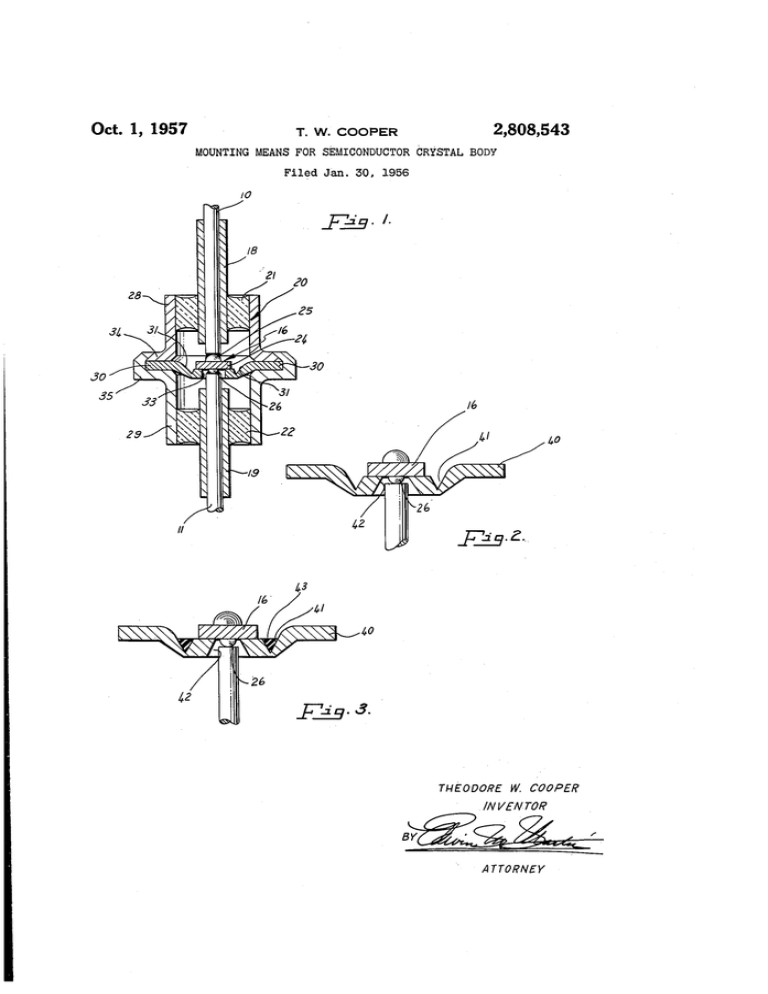
Fig. 1 is a sectional viewof anillustrative junctionltype
transistor in which the semiconductorttransistor body is 45 has a larger area than the emitter junction whichis gen
mounted upon a mounting diaphragm constructed in ac
erally desirable.
The semi-conductor crystal body is hermetically en
cordance with the present invention;
capsulated as disclosed in the copending application to
Fig. 2 is an alternativeembodiment of the mounting
diaphragm of thepresentinvention, shown not‘to scalefor
R. A. Gudmundsen and W. Waters, supra, by a?ixing
purposes of clarity; and
50 the semiconductor transistor body 16 ‘to the semicon
Fig. 3 is another alternative embodiment of the mount
ductor body mounting diaphragm 30 constructed in
ing diaphragm constructed‘inaccordance .with the‘present
accordance with vthe present invention. The mounting
diaphragm 30 ‘is a dish-shaped disc of electrically and
Referring now to the drawing, Fig. -1 ‘shows a fused
thermally conductive material which de?nes an opening
junctiontransistor of the type‘known'tothe art‘which is
33 symmetrical about'the centerline having a diameter
illustrative of the semiconductor devices .in which the
substantially less than the width of the transistor body
present invention may be advantageouslyiutilized. For
16 but greater than the diameter of the lead-arsenic
purposes of illustration, an N-P-Njunction transistor of
pellet 26 on the surface of-the germanium crystal body
the type disclosed and claimed'in‘the copending applica
which is to be the contact surface of the germanium
tion of Waters and Gudmundsen, supra,in-which germani
crystal body with the mounting diaphragm 30. The
um is utilized as the ‘semiconductor body will bedescribed
thickness of the mounting diaphragm is substantially
to show the utility and operation of the .presentinvention.
reduced along a diameter substantially greater than the
In addition, the ohmic connections toithe semiconductor
diameter of the opening.
transistor body are formedin- accordance with the copend
For example, in the presently perferred embodiment,
ing application Serial No. 550,317, vfor “Junction Type 65 the mounting diaphragm ‘30 is .a disheshaped disc of cold
Semiconductor Devices and Method of “Making the Same,”
rolled steel having a thickness of the order of 20 mils
by Theodore W. Cooper, ?led December. 1, 1955, and
and an outside diameter of approximately 0.280". The
assigned to the assignee of ‘the present application. It
diaphragm de?nes an opening symmetrical about the
will be recognized, however, that ‘the mounting diaphragm
centerline which is approximately 40 mils in diameter.
and the operational steps of assembly to ‘be‘described 70 A depression is formed in the diaphragm forming a cir
cular region 31 of reduced thickness which is substan
may be employed to'mount‘the ‘semiconductor crystal
body in P-N-P or’N-P-iN junction ‘transistors, ‘P~'N—‘P
tially conical .in cross-sectional con?guration, as shown
in Figs. v1, 2, and 3. The minimum thickness of the dia
or N-'-P—N,point contact ‘transistors, and semiconductor
phragm, that'is, at the apexof the conical depression
diodes‘ in'whichgermanium, silicon, or intermetallic semi
75 is ‘.of'the order ‘of 8.mils and is at a radius of about 90
conductors are‘ used asithe‘semiconductor‘ body. j
invention.
‘
-
2,808,543
-
5
mils. In the present embodiment, the diaphragm is
formed by a punch press operation although many
methods of forming will be apparent to those skilled in
the art. Although a dish-shaped disc is utilized in this
embodiment, and is preferable, a planar disc having an
opening therethrough and a region of reduced thickness
surrounding the opening may also be used.
In accordance with Waters and Gudmundsen, supra,
gold paste, solder, or other thermally conductive material
is used to a?ix the transistor body 16 to the diaphragm 10
30 such that the center lines of the emitter and collector
junctions are substantially coincident with the longitu
dinal center line of the diaphragm. The encapsulating
package 20 for the transistor comprises a ?rst body por
tion 28 and a second body portion 29 which are hollow
cylinders of thermally conductive material having open
ends and an outwardly directed right angle ?ange 34, 35
at one end thereof. The ?ange 34 of the ?rst body por
tion 28 is substantially equal in outside diameter to the
_
_
_
6
.
.
.
transistor body extends beneath the upper surface of the
mounting diaphragm into the opening 33 through the
diaphragm, but is not in contact with the diaphragm.
With the semiconductor crystal body a?ixed to the mount
ing diaphragm, the ?rst and second body portions 28, 29
of the envelope are mated with the mounting diaphragm
36 positioned between the ?anges, and the device is as
sembled and sealed :by crimping the ?ange 35 over the
?ange 34 and the diaphragm 30. The ?anges are mated
and joined in such a way that a hermetic seal is obtained
between the respective body portions.
‘
The assembly of the transistor device is then com
pleted and an ohmic contact is obtained at the collector
and emitter junctions by heating the tubular members
18, 19, and the contact electrodes 10, 11 to a temperature
above the melting point of the solder. After the solder
becomes molten, the contact electrodes are advanced to
the position at which electrical contact is obtained between
the contact electrodes and the emitter 26 and collector 25
outside diameter of the diaphragm 30. However, the 20 pellets, respectively. After ohmic connection has been
?ange 35 of the second body portion 29 is substantially
determined electrically, the contact electrodes are further
greater in outside diameter than the ?ange of the ?rst
advanced a predetermined amount to provide a relatively
body portion by an amount su?‘icient to allow crimping
of the second ?ange 35 over the diaphragm 30 and the
?rst ?ange 34 as shown. The diaphragm 30 and the‘ ?rst
and second body portions 28, 29 may be formed of cold
rolled steel.
Although the semiconductor body mounting diaphragm
30 of the present invention is not limited to the encapsu
lating means described, such encapsulating means have
large area of ohmic contact between the electrodes and the
lead oxide pellets, and the ?nal seal of the device is
formed.
Thus, in use, shocks and stresses upon the en
capsulating envelope are isolated from the area of the
semiconductor crystal body since stresses are relieved and
shocks absorbed in the region of reduced thickness of the
diaphragm where deformation may most easily occur.
Referring now to Fig. 2, an alternative embodiment of
given excellent results in combination with the present
the mounting diaphragm of the present invention is shown.
invention. Although the contact electrodes 10, 11 in
A circular depression 41 similar to that shown and de
an encapsulated semiconductor transistor of the type
scribed in connection with Fig. l is formed in the mount
shown in Fig. 1 may be mounted and positioned in the
ing diaphragm 40 which de?nes an opening 42 through
encapsulating device by methods known to the art, the 35 the diaphragm symmetrically about the longitudinal cen
methods of mounting and positioning the electrodes dis
terline of the diaphragm 40. The opening 42 through
closed in the copending application to Cooper, supra,
the diaphragm is frusto-conical in con?guration. The
has been found to be particularly advantageous. Accord
frusto-conical opening 42 has its major diameter at the
ingly, the production of such a semiconductor transistor
surface of the diaphragm opposed to the surface upon
device utilizing the contact electrode mounting method 40 which the semiconductor crystal body 16 is mounted.
disclosed in Cooper, supra, together with the encapsulat
Thus, in the case of a transistor in which it is desirable
to have the region of contact extend as close as possible
ing means described and claimed in Waters and Gudmund
to the lead-arsenic emitter pellet 26 and thus the N-type
sen, supra, will be described as illustrative in connection
region for purposes of reducing base resistance and in
with the utilization of a semiconductor crystal body
mounting diaphragm in accordance with the present
creasing thermal conduction, it still remains possible to
invention.
make the ohmic connection to the emitter pellet with rela
tive ease.
The electrodes 10, 11 are inserted into the tubular
members 18, 19 after being pretinned in order to furnish
Referring now to Fig. 3, when the amount of heat to be
conducted away from the crystal body is su?iciently great
the necessary amount of solder to ?ll the body between
the outside surface of the electrode and the inside sur 50 that the decreased thickness of the diaphragm causes a
face of the tubular member. The ?rst tubular member
18 and the second tubular member 19 are positioned
proximate the respective emitter and collector areas to
which the ohmic connections are to be made by extend
heat conduction problem, it is found to be advantageous
to ?ll the depression 41 with a malleable metal 43 which
is thermally conductive. Thus, deformation of the dia
phragm and isolation of the semiconductor crystal body
ing the tubular members 13, 19 through the encapsula 55 from excessive stresses and shocks is still provided al
tion means while electrically insulating them therefrom.
though the heat conduction path has not been reduced.
In this embodiment, the tubular members 18, 19 are
Thus, the present invention provides a means for mount
formed of iron-nickel alloy and are of the order of 0.06”
ing a semiconductor crystal body in an encapsulated semi
in outside diameter with an inside diameter of the order
conductor device which isolates the region of the dia
of 0.3”. For production purposes it has been found 60 phragm upon which the semiconductor crystal body is
advantageous to ai?x and seal the tubular members Within
mounted from excessive stresses, shocks, and strains to
the body portions by using a sintered glass insulative
bond in the form of glass beads 21, 22 surrounding each
which the encapsulating envelope may be subjected.
tact electrodes 10, 11 positioned in the respective tubular
cal about the axis of said diaphragm, said opening having
What is claimed is:
member which is formed under high pressure to eifect
1. In an encapsulated semiconductor device, means for
the insulative seal. in the production of a transistor the 65 mounting and positioning a semiconductor crystal body
?rst and second tubular members 18, 19 are insulatively
comprising: a disc-shaped diaphragm, said diaphragm be
a?ixed and sealed within the ?rst and second body por
ing electrically and thermally conductive, said diaphragm
tions 23, 29, respectively, with the ?rst and second con
de?ning an opening therethrough substantially symmetri
members. The space between the inside surface of the 70 an area substantially less than a contact surface of said
tubular members and the outside surface of the contact
semiconductor crystal body, said diaphragm de?ning a re
electrodes is ?lled with solder.
gion of reduced thickness surrounding said opening; said
The semiconductor transistor body 16 is mounted upon
semiconductor crystal body being ohmically a?’ixed to
the mounting diaphragm 30 such that the lead-arsenic pel
said diaphragm symmetrical with respect to said axis.
let 26 de?ning the emitter region of the semiconductor 75 2. In an encapsulated semiconductor device, means for
2,808.5é8
4. In an encapsulated semiconductor transistor device,
means for mounting and positioning a semiconductor
' mounting and positioning a semiconductor crystal body
comprising: a diaphragm, said diaphragm ‘being a dish
transistor ‘body "having tP-N junctions at ?rst and second
shaped disc of thermally conductive material, said dia
phragm de?ning an opening therethrough symmetrical
opposed surfaces thereof, comprising’: a transistor body
mounting diaphragm, said diaphragm being a dish-shaped
disc of electrically and thermally conductive material,
said diaphragm de?ning an opening therethrough sym
metrical about the axis of said diaphragm, said opening
about the axis of said diaphragm, said opening having an
area substantially ‘less than a contact surface of said
semiconductor crystal body, said diaphragm de?ning a
region of reduced thickness surrounding said opening at
having an area substantially less than the area of said
a diameter substantially greater than the diameter of said
opening; said semiconductor crystal body being ohmically
a?ixed to said diaphragm symmetrical with respect vto said
axis.
3. In an encapsulated semiconductor device, means for
mounting and positioning a semiconductor crystal ‘body
comprising: a semiconductor crystal body mounting dia
phragm, said diaphragm being a dish-‘shaped disc of elec
trically and thermally conductive material, said diaphragm
de?ning a circular opening therethrough symmetrical
about the axis of said diaphragm, said opening having
an area substantially ‘less than a contact surface of said
semiconductor crystal body, said diaphragm de?ning a
regiontof reduced thickness surrounding said opening at
a diameter substantially greater than the diameter of said
opening, said region of reduced thickness being provided
by a groove having a substantial depth; said semiconductor
crystal body being ohmically a?ixed‘ to said diaphragm
symmetrically with respect to said axis.
10
?rst surface of said transistor body and greater than the
P-N junction region at said ?rst surface; said diaphragm
de?ning a region of reduced thickness surrounding said
opening at a diameter substantially greater than the diam
eter of said opening, said region of reduced thickness
being a groove having a substantial depth; said transistor
body being ohmically affixed to said diaphragm symmetri
cal with respect to said axis within the area enclosed by
said groove, whereby said transistor body is isolated from
shocks and-stresses transmitted tosaid diaphragm.
ReferencesCitcd in the ?le of this patent
UNITED STATES PATENTS
2,754,455
2,794,942
Panltove _____________ _._ July 10, 1956
Cooper _______________ __ June 4, 1957
