pdf version of this article
The Simulation of a High Gain InP/InGaAs/InP Double HBT with Varying Doping Profile Provided by ASCII User
Defined External Files within the ATLAS Framework
1.0 Introduction
A PN junction is formed when a P-type doped portion of a semiconductor is joined with a N-type doped portion.
The PN junction forms the basic unit of a bipolar transistor
[1] and is a fundamental component for functions such as rectification. If both the P-type and the N-type regions are comprised of the same semiconductor material, the junction is called a homojunction, used for many years in the form of bi-polar junction transistors
(homojunction BJTs) [1]. After many iterations and decades of development and improvement, the most innovative change is the replacement of the homojunction emitter material with larger energy gap material.
It is possible to now create new heterojunction and double heterojunction bipolar transistors [2] utilizing junction layers made of different heterojunction semiconductor materials. Typically a heterojunction bipolar transistor
(HBT) consists of a hetrojunction at the base-emitter junction and a homojunction at the base-collector junction.
A double hetrojunction bipolar transistor (DHBT) is made of two heterojunctions, both at the base-emitter and at base-collector junctions. These developments have lead to HBTs and DHBTs of such superior quality and performance that they are now commonplace in areas of electronic commerce.
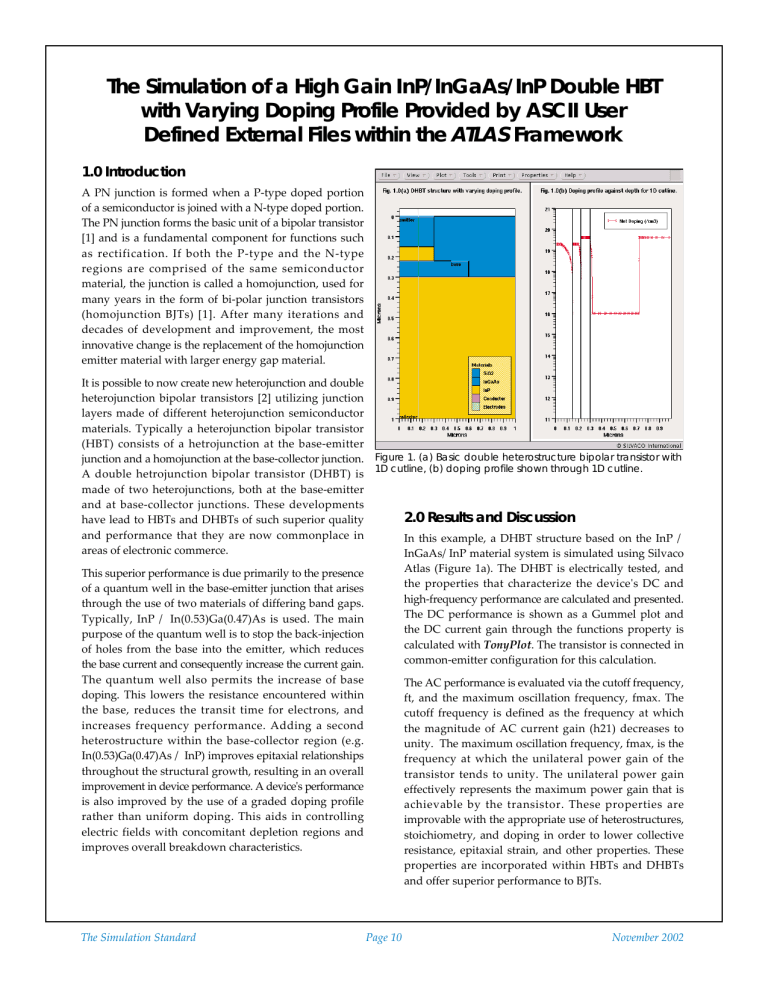
Figure 1. (a) Basic double heterostructure bipolar transistor with
1D cutline, (b) doping profile shown through 1D cutline.
This superior performance is due primarily to the presence of a quantum well in the base-emitter junction that arises through the use of two materials of differing band gaps.
Typically, InP / In(0.53)Ga(0.47)As is used. The main purpose of the quantum well is to stop the back-injection of holes from the base into the emitter, which reduces the base current and consequently increase the current gain.
The quantum well also permits the increase of base doping. This lowers the resistance encountered within the base, reduces the transit time for electrons, and increases frequency performance. Adding a second heterostructure within the base-collector region (e.g.
In(0.53)Ga(0.47)As / InP) improves epitaxial relationships throughout the structural growth, resulting in an overall improvement in device performance. A device's performance is also improved by the use of a graded doping profile rather than uniform doping. This aids in controlling electric fields with concomitant depletion regions and improves overall breakdown characteristics.
2.0 Results and Discussion
In this example, a DHBT structure based on the InP /
InGaAs/InP material system is simulated using Silvaco
Atlas (Figure 1a). The DHBT is electrically tested, and the properties that characterize the device's DC and high-frequency performance are calculated and presented.
The DC performance is shown as a Gummel plot and the DC current gain through the functions property is calculated with TonyPlot. The transistor is connected in common-emitter configuration for this calculation.
The AC performance is evaluated via the cutoff frequency, ft, and the maximum oscillation frequency, fmax. The cutoff frequency is defined as the frequency at which the magnitude of AC current gain (h21) decreases to unity. The maximum oscillation frequency, fmax, is the frequency at which the unilateral power gain of the transistor tends to unity. The unilateral power gain effectively represents the maximum power gain that is achievable by the transistor. These properties are improvable with the appropriate use of heterostructures, stoichiometry, and doping in order to lower collective resistance, epitaxial strain, and other properties. These properties are incorporated within HBTs and DHBTs and offer superior performance to BJTs.
The Simulation Standard Page 10 November 2002
n.type ascii infile=hbtex08_n doping x.min=0.0 x.max=1.0 y.min=0.0 y.max=1.0
p.type ascii infile=hbtex08_p invoke ASCII files previously written to specify the doping profiles. A correct h21 calculation is dependent on the careful consideration of device connections. This is achieved with the inport and outport commands, and then through solving for electrode voltages.
log outf=hbtex08_freq.log gains inport=base outport=collector width=50
Figure 2. Simulated DC current gain versus base voltage.
This example also demonstrates the import of doping profiles previously specified in an ASCII text editor.
These files are called upon during the simulation stage and the doping profiles are replicated accordingly. In this example, the files used are hbtex08_n and hbtex08_p for N-type and P-type doping, respectively.
The user simply creates an ASCII text file containing two columns. The left column specifies the depth location and the right column specifies the concentration at that location.
An example would be:
0.0
1.0
1e16
1e20
1.001
0.0
2.0
0.0
<Must put a carriage return here>
ASCII text file contain no metadata and require a carriage return at the end of the file. These commands make use of the ASCII file: doping <specify type> ascii infile=<filename> solve v2=1.0 v3=1.0 vstep=0.025 electrode=23 ac freq=1e7.
In this example, electrode 2 is the base and electrode 3 is the collector. The current gain is calculated from the ratio of Ic/Ib at DC and is designed to have a value in excess of 100 (Figure 2). The high frequency performance is satisfactory with operating frequencies in excess of 1e9Hz and gives reasonable ft and fmax as shown in Figures 3a and 3b, respectively.
3.0 Conclusions
In this report, a high gain double heterojunction bipolar transistor (DHBT) is simulated and evaluated using
ATLAS . It demonstrates that satisfactory results are easily achieved and specifies complicated doping profiles.
These profiles are defined by the user with ASCII text files and are invoked during runtime to achieve desired effects on the electrical characteristics.
References
[1] Shockley W., ‘The theory of p-n junctions in semiconductors and p-n junction transistors", Bell Syst. Tech.,
J., Vol 28, p435 (1949).
[2] Shockley W., U.S. Patent 2, 569, 347 (1951).
Interpolation is used between specified the locations.
Consequently, the doping profile must be set to zero at certain locations if so desired. If they are not, an interpolated value is used until the end of the device is encountered. For this example, complicated doping profiles are used throughout the structure (Figure 1b).
The profile should match with the 1D cutline in Figure 1a.
The input deck is written in the Silvaco’s DeckBuild environment in order to simulate the device and to evaluate its performance using specific commands. In this example, the commands: doping x.min=0.0 x.max=1.0 y.min=0.0 y.max=1.0
Figure 3. (a) Current gain against frequency. (b) Unilateral power gain against frequency.
November 2002 Page 11 The Simulation Standard

