Homework 2 Solution
advertisement
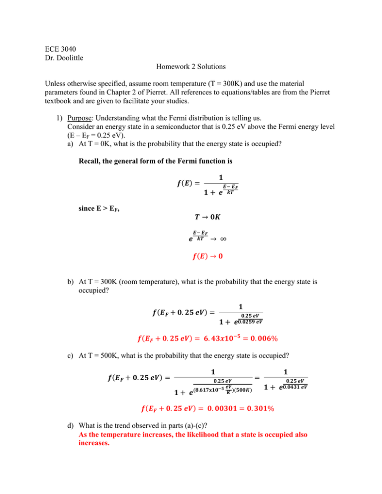
ECE 3040 Dr. Doolittle Homework 2 Solutions Unless otherwise specified, assume room temperature (T = 300K) and use the material parameters found in Chapter 2 of Pierret. All references to equations/tables are from the Pierret textbook and are given to facilitate your studies. 1) Purpose: Understanding what the Fermi distribution is telling us. Consider an energy state in a semiconductor that is 0.25 eV above the Fermi energy level (E – EF = 0.25 eV). a) At T = 0K, what is the probability that the energy state is occupied? Recall, the general form of the Fermi function is 𝒇(𝑬) = since E > EF, 𝒆 𝟏 𝟏+ 𝒆 𝑬− 𝑬𝑭 𝒌𝑻 𝑻 → 𝟎𝑲 𝑬− 𝑬𝑭 𝒌𝑻 → ∞ 𝒇(𝑬) → 𝟎 b) At T = 300K (room temperature), what is the probability that the energy state is occupied? 𝒇(𝑬𝑭 + 𝟎. 𝟐𝟓 𝒆𝑽) = 𝟏 𝟎.𝟐𝟓 𝒆𝑽 𝟏 + 𝒆𝟎.𝟎𝟐𝟓𝟗 𝒆𝑽 𝒇(𝑬𝑭 + 𝟎. 𝟐𝟓 𝒆𝑽) = 𝟔. 𝟒𝟑𝒙𝟏𝟎−𝟓 = 𝟎. 𝟎𝟎𝟔% c) At T = 500K, what is the probability that the energy state is occupied? 𝒇(𝑬𝑭 + 𝟎. 𝟐𝟓 𝒆𝑽) = 𝟏+ 𝟏 𝟎.𝟐𝟓 𝒆𝑽 −𝟓 𝒆𝑽 𝒆(𝟖.𝟔𝟏𝟕𝐱𝟏𝟎 𝑲 )(𝟓𝟎𝟎𝑲) = 𝟏 𝟎.𝟐𝟓 𝒆𝑽 𝟏 + 𝒆𝟎.𝟎𝟒𝟑𝟏 𝒆𝑽 𝒇(𝑬𝑭 + 𝟎. 𝟐𝟓 𝒆𝑽) = 𝟎. 𝟎𝟎𝟑𝟎𝟏 = 𝟎. 𝟑𝟎𝟏% d) What is the trend observed in parts (a)-(c)? As the temperature increases, the likelihood that a state is occupied also increases. 2) Purpose: Understanding the electron distribution in the conduction band. Consider a semiconductor with a Fermi level that lays 5kT below the conduction band. Assume the sample is held at room temperature. Which of the following energy levels holds more free electrons? A) E1 = EC + 1/4kT B) E2 = EC + 10kT Explain. Density of States function in the conduction band: 𝒈𝑪 (𝑬) = Fermi function: 𝒇(𝑬) = 𝒎∗𝒏 �𝟐𝒎∗𝒏 (𝑬 − 𝑬𝑪 ) 𝝅𝟐 ℏ𝟑 𝟏 𝑬− 𝑬𝑭 𝟏+ 𝒆 𝒌𝑻 Electron concentration at a given energy: 𝒎∗𝒏 �𝟐𝒎∗𝒏 (𝑬 − 𝑬𝑪 ) 𝑵(𝑬) = 𝒈𝑪 (𝑬)𝒇(𝑬) = 𝝅 𝟐 ℏ𝟑 𝟏 𝟏+ 𝒆 𝑬− 𝑬𝑭 𝒌𝑻 To obtain the number of free electrons at any given energy E above the conduction band energy EC, we must use the above formula. Luckily, in this case, some simplifications can be made. 1) Since we are only comparing two electron concentrations at different energies in the same semiconductor, we can neglect the constant terms in the Density of States expression (they are the same in both cases). 2) Since the Fermi energy is more than 3kT below the conduction band energy, we can employ the Boltzmann approximation, 𝒇(𝑬) = Sections 2.4.2 and 2.4.3 in Pierret. 𝑵(𝑬) = 𝒈𝑪 (𝑬)𝒇(𝑬) ∝ �(𝑬 − 𝑬𝑪 ) 𝒆 Energy 1: 𝑵 �𝑬𝑪 + Energy 2: 𝟏 𝑬− 𝑬𝑭 𝒆 𝒌𝑻 = 𝒆 𝑬𝑭 −𝑬 𝒌𝑻 , as detailed in 𝑬𝑭 −𝑬 𝒌𝑻 −𝟓.𝟐𝟓𝒌𝑻 𝟏 𝟏 𝒌𝑻� ∝ � 𝒌𝑻 𝒆 𝒌𝑻 = �(𝟎. 𝟐𝟓)(𝟎. 𝟎𝟐𝟓𝟗 𝒆𝑽) 𝒆−𝟓.𝟐𝟓 𝟒 𝟒 = 𝟒. 𝟐𝟐𝟑𝐱𝟏𝟎−𝟒 𝒆𝑽 𝑵(𝑬𝑪 + 𝟏𝟎𝒌𝑻) ∝ √𝟏𝟎𝒌𝑻 𝒆 −𝟏𝟓𝒌𝑻 𝒌𝑻 𝟏� 𝟐 = �(𝟏𝟎)(𝟎. 𝟎𝟐𝟓𝟗 𝒆𝑽) 𝒆−𝟏𝟓 = 𝟏. 𝟓𝟓𝟕𝐱𝟏𝟎−𝟕 𝒆𝑽 𝟏� 𝟐 Based on the above results, we know that Energy 1 will contain more free electrons than Energy 2. 3) Purpose: Understanding special cases of doping. Concentration questions with a twist. a) At room temperature, the hole concentration in a piece of silicon is 1016 cm-3. What is the electron concentration? Since we already know p = 1016 cm-3, we can use the np product rule to obtain n: 𝒏𝒑 = 𝒏𝟐𝒊 The intrinsic concentration of silicon is 1010 cm-3. 𝒏= 𝒏= 𝒏𝟐𝒊 𝒑 (𝟏𝟎𝟏𝟎 𝒄𝒎−𝟑 )𝟐 𝟏𝟎𝟐𝟎 𝒄𝒎−𝟔 = 𝟏𝟎𝟏𝟔 𝒄𝒎−𝟑 𝟏𝟎𝟏𝟔 𝒄𝒎−𝟑 𝟒 −𝟑 𝒏 = 𝟏𝟎 𝒄𝒎 b) For a silicon sample maintained at room temperature, the Fermi level is 4kT below the intrinsic Fermi level. What are the carrier concentrations? We can use Equations 2.19a and 2.19b to directly solve for n and p. (𝑬𝑭 −𝑬𝒊 ) � 𝒌𝑻 (𝑬𝒊 −𝑬𝑭 ) � 𝒌𝑻 𝒏𝒊 𝒆 𝒏 = 𝒏𝒊 𝒆 𝒑= (−𝟒𝒌𝑻 ) � 𝒌𝑻 𝒏 = (𝟏𝟎𝟏𝟎 𝒄𝒎−𝟑 )𝒆 𝟖 −𝟑 𝒏 = 𝟏. 𝟖𝟑𝐱𝟏𝟎 𝒄𝒎 (+𝟒𝒌𝑻 ) � 𝒌𝑻 𝒑 = (𝟏𝟎𝟏𝟎 𝒄𝒎−𝟑 )𝒆 𝟏𝟏 −𝟑 𝒑 = 𝟓. 𝟒𝟔𝐱𝟏𝟎 𝒄𝒎 Alternatively, we can solve for either n or p using the above equations, and then employ the np product rule to obtain the other concentration. c) A silicon wafer is doped with NA = 1016 cm-3 and ND = 1018 cm-3. At T = 0K, what are the equilibrium electron and hole concentrations? Regardless of doping concentrations, at T = 0K, the semiconductor is in the “freeze-out” region. No donors or acceptors are ionized, and n = p = 0 cm-3 d) At elevated temperatures, a silicon wafer has carrier concentrations n = p = 1019 cm-3. Can we tell what the dopant concentration is? No, we cannot tell anything from the above statement. Depending on how high the temperature is, the semiconductor can be in the “intrinsic temperature” region. In this region, so much thermal energy is applied to the system that bound electrons in the valence band are promoted over the entire bandgap and become free electrons in the conduction band, leaving behind holes in the valence band, overpowering any doping effects. e) Using Table 2.1 and knowing that the bandgap of GaAs is 1.43 eV, show that the intrinsic carrier concentration of GaAs is 2x106 cm-3. Strategy: Determine Density of States in the conduction band and valence band (NC and NV), and use these values and the known bandgap to determine the intrinsic concentration. From Table 2.1, the effective masses of electrons and holes in GaAs are: 𝒎∗𝒏 = 𝟎. 𝟎𝟔𝟔𝒎𝟎 𝒎∗𝒑 = 𝟎. 𝟓𝟐𝒎𝟎 Using Equations 2.13a and 2.13b: 𝟑 𝒎∗𝒏 𝒌𝑻 �𝟐 𝟑 𝑵𝑪 = 𝟐 � � = (𝟐. 𝟓𝟏𝟎𝐱𝟏𝟎𝟏𝟗 𝒄𝒎−𝟑 )(𝒎∗𝒏 ⁄𝒎𝟎 ) �𝟐 𝟐 𝟐𝝅ℏ 𝟑 𝑵𝑪 = (𝟐. 𝟓𝟏𝟎𝐱𝟏𝟎𝟏𝟗 𝒄𝒎−𝟑 )(𝟎. 𝟎𝟔𝟔) �𝟐 = 𝟒. 𝟐𝟔𝐱𝟏𝟎𝟏𝟕 𝒄𝒎−𝟑 𝒎∗𝒑 𝒌𝑻 𝑵𝑽 = 𝟐 � � 𝟐𝝅ℏ𝟐 𝟑� 𝟐 = (𝟐. 𝟓𝟏𝟎𝐱𝟏𝟎𝟏𝟗 𝒄𝒎−𝟑 )�𝒎∗𝒑 ⁄𝒎𝟎 � 𝑵𝑽 = (𝟐. 𝟓𝟏𝟎𝐱𝟏𝟎𝟏𝟗 𝒄𝒎−𝟑 )(𝟎. 𝟓𝟐) Using Equation 2.21: 𝟑� 𝟐 𝟑� 𝟐 = 𝟗. 𝟒𝟏𝐱𝟏𝟎𝟏𝟖 𝒄𝒎−𝟑 𝒏𝒊 = �𝑵𝑪 𝑵𝑽 𝒆−𝑬𝑮⁄𝟐𝒌𝑻 𝒏𝒊 = �(𝟒. 𝟐𝟔𝐱𝟏𝟎𝟏𝟕 𝒄𝒎−𝟑 )(𝟗. 𝟒𝟏𝐱𝟏𝟎𝟏𝟖 𝒄𝒎−𝟑 )𝒆−𝟏.𝟒𝟑 𝒆𝑽⁄𝟎.𝟎𝟓𝟏𝟖 𝒆𝑽 𝒏𝒊 = 𝟐. 𝟎𝟓𝐱𝟏𝟎𝟔 𝒄𝒎−𝟑 4) Purpose: Understanding the energy band diagram. Draw the energy band diagram of a hypothetical semiconductor with the following properties: • T = 300K • m*n = 0.7m0 • m*p = 0.3m0 • EG = 1.2 eV • n = 1013 cm-3 On your diagram, label EG, EC, EV, EF and Ei and note their values. Hint: Do not assume that Ei is at mid-gap. Strategy: Determine Ei with the given effective masses. Then determine Density of States in the conduction and valence bands, NV and NC, using the effective masses. Use these values to determine the intrinsic concentration of the semiconductor. Use the intrinsic concentration of the semiconductor and the given electron concentration to determine EF. Draw all relevant energy levels on a diagram, using the valence band energy as a reference (EV = 0 eV). Using Equation 2.36: 𝒎∗𝒑 𝒎∗𝒑 𝑬𝑪 + 𝑬𝑽 𝟑 𝑬𝑮 𝟑 𝑬𝒊 = + 𝒌𝑻 𝐥𝐧 � ∗ � = + 𝒌𝑻 𝐥𝐧 � ∗ � 𝟐 𝒎𝒏 𝟐 𝒎𝒏 𝟒 𝟒 𝟏. 𝟐 𝒆𝑽 𝟑 𝟎. 𝟑 𝑬𝒊 = + 𝒌𝑻 𝐥𝐧 � � = 𝟎. 𝟓𝟖𝟒 𝒆𝑽 𝟐 𝟒 𝟎. 𝟕 Using Equations 2.13a and 2.13b: 𝟑 𝒎∗𝒏 𝒌𝑻 �𝟐 𝟑 𝑵𝑪 = 𝟐 � � = (𝟐. 𝟓𝟏𝟎𝐱𝟏𝟎𝟏𝟗 𝒄𝒎−𝟑 )(𝒎∗𝒏 ⁄𝒎𝟎 ) �𝟐 𝟐 𝟐𝝅ℏ 𝟑 𝑵𝑪 = (𝟐. 𝟓𝟏𝟎𝐱𝟏𝟎𝟏𝟗 𝒄𝒎−𝟑 )(𝟎. 𝟕) �𝟐 = 𝟏. 𝟒𝟕𝐱𝟏𝟎𝟏𝟗 𝒄𝒎−𝟑 𝒎∗𝒑 𝒌𝑻 𝑵𝑽 = 𝟐 � � 𝟐𝝅ℏ𝟐 𝟑� 𝟐 = (𝟐. 𝟓𝟏𝟎𝐱𝟏𝟎𝟏𝟗 𝒄𝒎−𝟑 )�𝒎∗𝒑 ⁄𝒎𝟎 � 𝑵𝑽 = (𝟐. 𝟓𝟏𝟎𝐱𝟏𝟎𝟏𝟗 𝒄𝒎−𝟑 )(𝟎. 𝟑) 𝟑� 𝟐 𝟑� 𝟐 = 𝟒. 𝟏𝟐𝐱𝟏𝟎𝟏𝟖 𝒄𝒎−𝟑 Using Equation 2.21: 𝒏𝒊 = �𝑵𝑪 𝑵𝑽 𝒆−𝑬𝑮⁄𝟐𝒌𝑻 𝒏𝒊 = �(𝟏. 𝟒𝟕𝐱𝟏𝟎𝟏𝟗 𝒄𝒎−𝟑 )(𝟒. 𝟏𝟐𝐱𝟏𝟎𝟏𝟖 𝒄𝒎−𝟑 )𝒆−𝟏.𝟐 𝒆𝑽⁄𝟎.𝟎𝟓𝟏𝟖 𝒆𝑽 𝒏𝒊 = 𝟔. 𝟕𝟔𝒙𝟏𝟎𝟖 𝒄𝒎−𝟑 Using Equation 2.19a: 𝒏 = 𝒏𝒊 𝒆 (𝑬𝑭 −𝑬𝒊 ) � 𝒌𝑻 𝒏 𝑬𝑭 = 𝑬𝒊 + 𝒌𝑻 𝐥𝐧 � � 𝒏𝒊 𝟏𝟎𝟏𝟑 𝒄𝒎−𝟑 𝑬𝑭 = 𝟎. 𝟓𝟖𝟒 𝒆𝑽 + (𝟎. 𝟎𝟐𝟓𝟗 𝒆𝑽) 𝐥𝐧 � � 𝟔. 𝟕𝟔𝐱𝟏𝟎𝟖 𝒄𝒎−𝟑 𝑬𝑭 = 𝟎. 𝟖𝟑𝟑 𝒆𝑽 5) Purpose: Understanding of electron-hole relationships. Consider a piece of silicon held at room temperature. For the various doping conditions, find the hole and electron concentrations, the Fermi level, and note whether the sample is n-type or p-type. Assume total ionization of dopants. a) 1017 cm-3 P From Table 2.2, we know that P (phosphorus) is a donor in silicon. Therefore, 𝑵𝑫 = 𝟏𝟎𝟏𝟕 𝒄𝒎−𝟑 𝑵𝑨 = 𝟎 𝒄𝒎−𝟑 𝑵𝑫 − 𝑵𝑨 = 𝑵𝑫 ≫ 𝒏𝒊 𝒏 ≅ 𝑵𝑫 𝒏 = 𝟏𝟎𝟏𝟕 𝒄𝒎−𝟑 𝒑= (𝟏𝟎𝟏𝟎 𝒄𝒎−𝟑 )𝟐 𝒏𝟐𝒊 = 𝑵𝑫 𝟏𝟎𝟏𝟕 𝒄𝒎−𝟑 𝒑 = 𝟏𝟎𝟑 𝒄𝒎−𝟑 Approximating Ei as being at mid-gap, 𝒏 𝑬𝑮 𝒏 + 𝒌𝑻 𝐥𝐧 � � 𝑬𝑭 = 𝑬𝒊 + 𝒌𝑻 𝐥𝐧 � � = 𝒏𝒊 𝟐 𝒏𝒊 𝟏. 𝟏𝟐 𝒆𝑽 𝟏𝟎𝟏𝟕 𝒄𝒎−𝟑 + (𝟎. 𝟎𝟐𝟓𝟗 𝒆𝑽) 𝐥𝐧 � 𝟏𝟎 � 𝑬𝑭 = 𝟐 𝟏𝟎 𝒄𝒎−𝟑 𝑬𝑭 = 𝟎. 𝟗𝟗𝟕 𝒆𝑽 Sample is n-type. b) 1014 cm-3 P and 1018 cm-3 B From Table 2.2, we know that P is a donor in silicon and B (boron) is an acceptor in silicon. Therefore, 𝑵𝑫 = 𝟏𝟎𝟏𝟒 𝒄𝒎−𝟑 𝑵𝑨 = 𝟏𝟎𝟏𝟖 𝒄𝒎−𝟑 𝑵𝑨 − 𝑵𝑫 ≅ 𝑵𝑨 ≫ 𝒏𝒊 𝒑 ≅ 𝑵𝑨 = 𝟏𝟎𝟏𝟖 𝒄𝒎−𝟑 𝒏= (𝟏𝟎𝟏𝟎 𝒄𝒎−𝟑 )𝟐 𝒏𝟐𝒊 = 𝑵𝑨 𝟏𝟎𝟏𝟖 𝒄𝒎−𝟑 𝒏 = 𝟏𝟎𝟐 𝒄𝒎−𝟑 𝒑 𝑬𝑮 𝒑 𝑬𝑭 = 𝑬𝒊 − 𝒌𝑻 𝐥𝐧 � � = + 𝒌𝑻 𝐥𝐧 � � 𝒏𝒊 𝒏𝒊 𝟐 𝟏𝟖 𝟏. 𝟏𝟐 𝒆𝑽 𝟏𝟎 𝒄𝒎−𝟑 𝑬𝑭 = − (𝟎. 𝟎𝟐𝟓𝟗 𝒆𝑽) 𝐥𝐧 � 𝟏𝟎 � 𝟐 𝟏𝟎 𝒄𝒎−𝟑 𝑬𝑭 = 𝟎. 𝟎𝟖𝟑 𝒆𝑽 Sample is p-type. c) 1012 cm-3 As and 9x1011 cm-3 B From Table 2.2, As (arsenic) is a donor in silicon and B is an acceptor. Therefore, 𝑵𝑫 = 𝟏𝟎𝟏𝟐 𝒄𝒎−𝟑 𝑵𝑨 = 𝟗𝐱𝟏𝟎𝟏𝟏 𝒄𝒎−𝟑 This is a case of a “compensated” semiconductor, where ND and NA are comparable and nonzero. No simplifications can be made, and we need to carry both terms in our calculations. Using Equation 2.29a, 𝑵𝑫 − 𝑵 𝑨 𝑵𝑫 − 𝑵𝑨 𝟐 𝒏= + �� � + 𝒏𝟐𝒊 � 𝟐 𝟐 𝟏𝟎𝟏𝟐 𝒄𝒎−𝟑 − 𝟗𝐱𝟏𝟎𝟏𝟏 𝒄𝒎−𝟑 𝒏= 𝟐 𝟏⁄𝟐 𝟐 𝟏𝟎𝟏𝟐 𝒄𝒎−𝟑 − 𝟗𝐱𝟏𝟎𝟏𝟏 𝒄𝒎−𝟑 + �� � + (𝟏𝟎𝟏𝟎 𝒄𝒎−𝟑 )𝟐 � 𝟐 𝟏𝟎𝟏𝟏 𝒄𝒎−𝟑 + [𝟐. 𝟓𝐱𝟏𝟎𝟐𝟏 𝒄𝒎−𝟔 + 𝟏𝟎𝟐𝟎 𝒄𝒎−𝟔 ]𝟏⁄𝟐 = 𝟐 = 𝟓𝐱𝟏𝟎𝟏𝟎 𝒄𝒎−𝟑 + 𝟓. 𝟏𝟎𝐱𝟏𝟎𝟏𝟎 𝒄𝒎−𝟑 𝒏 = 𝟏. 𝟎𝟏𝐱𝟏𝟎𝟏𝟏 𝒄𝒎−𝟑 (𝟏𝟎𝟏𝟎 𝒄𝒎−𝟑 )𝟐 𝒏𝟐𝒊 𝒑= = 𝒏 𝟏. 𝟎𝟏𝐱𝟏𝟎𝟏𝟏 𝒄𝒎−𝟑 𝒑 = 𝟗. 𝟗𝟎𝐱𝟏𝟎𝟖 𝒄𝒎−𝟑 𝒏 𝑬𝑮 𝒏 + 𝒌𝑻 𝐥𝐧 � � 𝑬𝑭 = 𝑬𝒊 + 𝒌𝑻 𝐥𝐧 � � = 𝒏𝒊 𝟐 𝒏𝒊 𝟏. 𝟏𝟐 𝒆𝑽 𝟏. 𝟎𝟏𝐱𝟏𝟎𝟏𝟏 𝒄𝒎−𝟑 𝑬𝑭 = + (𝟎. 𝟎𝟐𝟓𝟗 𝒆𝑽) 𝐥𝐧 � � 𝟐 𝟏𝟎𝟏𝟎 𝒄𝒎−𝟑 𝑬𝑭 = 𝟎. 𝟔𝟐𝟎 𝒆𝑽 Sample is n-type. 𝟏⁄𝟐 6) Purpose: Understanding partial ionization. Find the electron and hole concentrations as well as the Fermi level position for a silicon sample with the following conditions. a) 1017 cm-3 As, 9.5x1016 cm-3 Ga Using the method outlined in the Homework 2 handout in Microsoft Excel: 𝑬𝑭 = 𝟎. 𝟖𝟗𝟐 𝒆𝑽 𝒏 ≅ 𝟒. 𝟕𝟔𝟑𝐱𝟏𝟎𝟏𝟓 𝒄𝒎−𝟑 𝒑 ≅ 𝟐. 𝟎𝟓𝟎𝐱𝟏𝟎𝟒 𝒄𝒎−𝟑 b) 1017 cm-3 P, 9.5x1016 cm-3 Ga 𝑬𝑭 = 𝟎. 𝟖𝟗𝟐 𝒆𝑽 𝒏 ≅ 𝟒. 𝟖𝟑𝟎𝐱𝟏𝟎𝟏𝟓 𝒄𝒎−𝟑 𝒑 ≅ 𝟐. 𝟎𝟐𝟏𝐱𝟏𝟎𝟒 𝒄𝒎−𝟑 c) Why is P a more commonly used donor than As? Because the binding energy of P lies closer to the conduction band than the binding energy of As, it is a more efficient donor.
