Applied Surface Science 224 (2004) 87–90
Segregation of boron to polycrystalline and single-crystal
Si1xyGexCy and Si1yCy layers
E.J. Stewart*, J.C. Sturm
Center for Photonics and Optoelectronic Materials, Department of Electrical Engineering,
Princeton University, Princeton, NJ 08544, USA
Abstract
Strong boron segregation to polycrystalline Si1xyGexCy alloys from Si has previously been reported [MRS Symp. Proc. 669
(2001) J6.9]. In this study, we investigate potential mechanisms for this effect. We find that comparable segregation also occurs
in both polycrystalline Si1yCy and single-crystal Si1xyGexCy, indicating neither Ge nor grain boundary effects are needed for
it to occur. In addition, the stability of the electrical properties of polycrystalline Si1xyGexCy with annealing suggests that
inactive B–C defects are not forming. Point defect gradients are presented as a mechanism consistent with the electrical data.
# 2003 Elsevier B.V. All rights reserved.
PACS: 68.55.Ln
Keywords: Boron; Segregation; Diffusion; Si1xyGexCy; Polycrystalline
1. Introduction
Understanding dopant transport in Si1xyGexCy
and Si1yCy alloys is important for the integration
of these materials in modern devices such as
MOSFETs and HBTs. Previously, it has been shown
that boron strongly segregates to polycrystalline
Si1xyGexCy layers from Si [1]. This effect is more
pronounced than previous reports of boron segregation
to single crystal Si1xGex [2,3], and increases with
increasing carbon content. It has been exploited to
make polycrystalline Si1xyGexCy-gated MOSFETs
with increased resistance to boron penetration compared to either poly Si or Si1xGex gated devices
[4]. This work examines the mechanism driving this
*
Corresponding author. Tel.: þ1-609-258-6624;
fax: þ1-609-258-1840.
E-mail address: estewart@princeton.edu (E.J. Stewart).
segregation. We show that a similar segregation effect
occurs in both polycrystalline Si1yCy (no Ge) and
single crystal Si1xyGexCy, indicating that neither
Ge, nor any polycrystalline effects (i.e. grain boundary
defects), are needed for it to occur. In addition, the
electrical properties of polycrystalline Si1xyGexCy
indicate that inactive B–C related defects are not
forming. We discuss point-defect gradients as a possible mechanism driving this segregation.
2. Segregation in Si1xyGexCy and Si1yCy
All structures used in this study were grown by
Rapid Thermal Chemical Vapor Deposition at temperatures between 625 8C and 750 8C, using SiCl2H2,
SiH4, and Si2H6 as silicon sources and GeH4, SiCH6,
and B2H6 as germanium, carbon, and boron sources,
respectively. Two polycrystalline Si1yCy (no Ge)
0169-4332/$ – see front matter # 2003 Elsevier B.V. All rights reserved.
doi:10.1016/j.apsusc.2003.08.044
88
E.J. Stewart, J.C. Sturm / Applied Surface Science 224 (2004) 87–90
.
BF2+ 50 keV 2x1014 cm-2
+
p poly Si
p+ Si
40nm
p+ poly Si0.99C0.01 25nm
i-poly
100nm
thermal oxide
p+ Si
100nm
i-Si0.8Ge0.2
15nm
p+ poly Si0.996C0.004 25nm
p+ Si
100nm
p+ poly Si
buffer
+
p poly Si
i-poly Si0.996C0.004 200nm
200nm
150nm
i-Si0.79Ge0.2C0.01 15nm
40nm
40nm
.
.
Si (100) substrate
Si (100) substrate
(b)
(a)
(c)
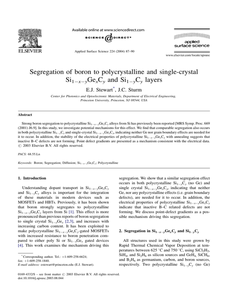
Fig. 1. Structures of: (a) two-layer polycrystalline Si/Si1yCy sample, (b) multi-layer poly Si/Si1yCy sandwich structure, and (c) singlecrystal multi-layer sandwich structure.
structures were fabricated, shown in Fig. 1 (a) and (b),
to study the importance of Ge in the segregation
process. Growth parameters for the Si1yCy layers
were chosen to incorporate carbon on substitutional
lattice sites [5]. The first structure consisted of 200 nm
of undoped poly Si1yCy underneath 100 nm of
undoped poly Si, all on a thermally oxidized Si
substrate. Boron was implanted into the top poly Si
layer by BF2þ at 2 1014 cm2 and 50 keV. To drive
the dopant into the underlying poly Si1yCy, a 900 8C,
4 h anneal was performed. Fig. 2 shows SIMS profiles
of this sample after the anneal. Boron has segregated
into the poly Si1yCy layer, with a segregation coefficient m ¼ ½Bpoly SiC =½Bpoly Si ¼ 1:5 (longer anneals
performed on similar poly Si/Si1xyGexCy structures
do not show any more increase in the segregation).
-3
poly Si poly Si0.996C0.004
10
19
+
14
Implant BF2 2x10 cm
-2
0
10
Anneal 900 C 4 hours
18
0
50
100
150
200
Boron concentration (cm )
20
-3
Boron concentration (cm )
10
This value is comparable to that of poly Si1xyGexCy
layers with similar C content, indicating that Ge is not
required for segregation.
The second sample was a multi layer structure that
included two poly Si1yCy (0.4% and 1%) layers
sandwiched between poly Si layers. This sample
was in situ doped with boron during growth at a
much higher level than the previous sample, 7 1020 cm3 . An 800 8C, 22 h anneal was performed to
allow for dopant redistribution, and SIMS profiles
taken before and after the anneal (Fig. 3). For the
0.4% layer, segregation is similar to the previous
sample, m ¼ 1:3. A larger effect is seen in the 1%
layer, with m ¼ 1:8. Again, segregation is observed
without Ge even at very high doping levels, and
increases with increasing carbon content.
250
300
Depth (nm)
Fig. 2. SIMS profile of implanted two-layer poly Si/Si0.996C0.004
sample, showing boron segregation to poly Si0.996C0.004 layer after
a 900 8C, 4 h anneal.
10
21
poly
Si0.99C0.01
0
anneal 800 C,
22 hours
as grown
10
poly
Si0.996C0.004
20
150
200
250
Depth (nm)
Fig. 3. SIMS profile of multi-layer in situ doped poly Si/Si1yCy
sandwich structure, showing increasing segregation at higher
carbon levels.
20
10
19
Si0.79Ge0.2C0.01
10
Si0.8Ge0.2
as-grown
0
anneal 800 C, 28 hours
18
100
200
300
Depth (nm)
Fig. 4. SIMS profile of single-crystal Si/Si1xyGexCy sandwich
structure, showing increased boron segregation into Si0.79Ge0.2C0.01
vs. Si0.8Ge0.2.
A third sample was grown to investigate segregation
in single crystal material, shown in Fig. 1(c). On top of
an n-type substrate and buffer, thin (15 nm) epitaxial
layers of undoped Si1xGex and Si1xyGexCy were
sandwiched between thicker (100 nm) doped Si
layers (½B ¼ 2 1019 cm3 ). This structure was
capped with deposited SiO2 and annealed at 800 8C
for 28 h to allow boron to move into the Si1xGex
and Si1xyGexCy layers. Fig. 4 shows SIMS of this
structure before and after annealing. The as-grown
profile shows a boron peak outside the Si1xyGexCy
layers at 20 nm, which was unintentionally incorporated during growth and should not have an effect on
the rest of the experiment. Boron segregation into the
Si1xGex layer (m ¼ 1:7) is observed as anticipated,
and comparable to reported values [2,3]. However,
additional segregation occurs in the Si1xyGexCy
layer (m ¼ 2:3), revealing that carbon also enhances
boron segregation in single-crystal material. Polycrystalline effects (i.e. grain boundary defects) are not
(at least completely) responsible for the previously
observed segregation to poly Si1xyGexCy.
FB ¼ DB
dð½BðI=I0 ÞÞ
dx
1.5x 10
-1
1.0x 10
-1
5.0x 10
-2
in-situ doped la yers
19
-3
[B ] ~ 1 0 cm
pol y S i
pol y S i0.79 Ge 0.2 C 0.01
po ly Si 0.796 Ge 0.2 C 0.004
0.0
3. Discussion
89
electronic energy differences due to the smaller band
gap of Si1xGex versus Si [6], and direct Ge–B interactions [7]. When small amounts of substitutional
carbon are added to Si1xGex commensurate on Si,
the carbon is known to lead to less macroscopic
strain and a larger band gap than Si1xGex, both of
which would predict less segregation of boron to
Si1xyGexCy layers. This is the opposite of what is
observed. In addition, the observation of segregation
to Si1yCy layers indicates that carbon itself can drive
the segregation, without any Ge–B effects.
Another possibility is that direct B–C interactions are
responsible. For example, Liu et al. proposed an immobile boron-carbon-interstitial cluster [8]. In this case,
one might expect to see a degradation of the electrical
properties upon annealing (assuming the B–C defects
render the boron inactive). Fig. 5 shows the resistivity of
polycrystalline Si1xyGexCy layers (compared to poly
Si and Si1xGex) annealed at 900 8C for a long time (all
layers were in situ doped at 1 1019 cm3 ). While
the as-grown poly Si1xyGexCy does have a higher
resistivity versus the poly Si1xGex, no increase is
observed during the anneal, even out to 24 h (much
longer than the time scale required to allow for segregation). This suggests that inactive defects are not
responsible for the segregation.
Point defect gradients represent another possible
driving mechanism. Boron diffusion in Si has been
shown to be mediated by Si interstitials. The equation
for boron diffusion flux can be expressed as [9]:
ρ (Ω-cm)
10
-3
Boron concentration (cm )
E.J. Stewart, J.C. Sturm / Applied Surface Science 224 (2004) 87–90
po ly Si 0.8 Ge 0.2
0
5
10
15
20
25
0
Several mechanisms have been proposed to explain
boron segregation in single-crystal strained Si1xGex
(no C) versus Si. These include relieving strain energy,
Anneal Time at 900 C (hours)
Fig. 5. Resistivity of in situ doped poly Si, poly Si1xGex, and poly
Si1xyGexCy layers vs. anneal time.
90
E.J. Stewart, J.C. Sturm / Applied Surface Science 224 (2004) 87–90
where FB is the diffusion flux of boron atoms, [B] is
the concentration of boron, DB is the equilibrium
diffusivity of boron, and I/I0 is the ratio of Si interstitials to the equilibrium value. If the interstitial
profile varies with position, the equation becomes:
I d½B
dðI=I0 Þ
DB ½B
FB ¼ DB
I0 dx
dx
The first term is the usual diffusion flux due to a
concentration gradient, while the second term represents a flux of boron atoms due to an interstitial
gradient, even if no gradient exists in the boron profile.
Si1xyGexCy and Si1yCy layers are known to locally
suppress the concentration of interstitials [10]. If the
interstitial concentration is decreased in a region, then
an additional driving force exists for boron to move to
that region, producing a segregation effect. As this
mechanism does not require the presence of inactive
B–C defects, it is consistent with the results of the
electrical measurements. Further experiments are
underway to confirm this conclusion.
4. Summary
In conclusion, we have investigated different
mechanisms to explain boron segregation in polycrystalline Si1xyGexCy alloys. Comparable effects are
seen in both polycrystalline Si1yCy and single crystal
Si1xyGexCy, indicating neither Ge nor grain boundary
effects are necessary. Stability of the electrical properties of polycrystalline Si1xyGexCy with annealing
suggests that inactive B–C related defects are not
forming. Point defect gradients are presented as a
mechanism consistent with the electrical data.
Acknowledgements
This work was supported by DARPA/ONR
N660001-97-8904 and ARO DAA655-98-1-0270.
References
[1] E.J. Stewart, M.S. Carroll, J.C. Sturm, MRS Symp. Proc. 669
(2001) J6.9.
[2] S.M. Hu, D.C. Ahlgren, P.A. Ronsheim, J.O. Chu, Phys. Rev.
Lett. 67 (1991) 1450–1453.
[3] T.T. Fang, W.T.C. Fang, P.B. Griffin, J.D. Plummer, Appl.
Phys. Lett. 68 (6) (1996) 791–793.
[4] E.J. Stewart, M.S. Carroll, J.C. Sturm, IEEE Electron Device
Lett. 22 (12) (2001) 574–576.
[5] M.S. Carroll, J.C. Sturm, Appl. Phys. Lett. 81 (7) (2002)
1225–1227.
[6] S.M. Hu, Phys. Rev. B 45 (8) (1992) 4498–4501.
[7] R.F. Lever, J.M. Bonar, A.F.W. Willoughby, J. Appl. Phys. 83
(4) (1998) 1988–1994.
[8] C.-L. Liu, W. Windl, L. Borucki, S. Lu, X.Y. Liu, Appl. Phys.
Lett. 80 (1) (2002) 52–54.
[9] C.S. Rafferty, H.-H. Vuong, S.A. Eshraghi, M.D. Giles, M.R.
Pinto, S.J. Hillenius, IEDM Tech. Digest (1993) 311–314.
[10] R. Scholz, U. Gosele, J-Y. Huhm, T.Y. Tan, Appl. Phys. Lett.
72 (2) (1998) 200–202.


