A 75 GHz Current Mode Logic Static Frequency Divider
advertisement
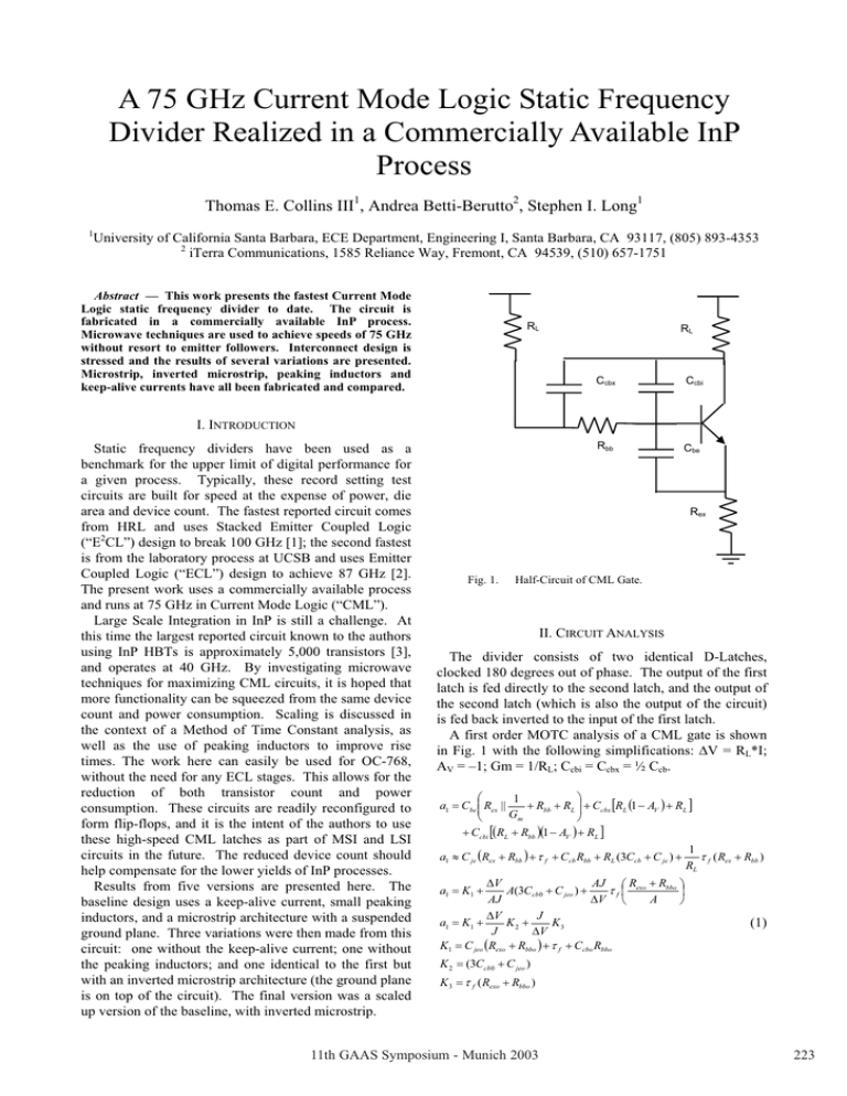
A 75 GHz Current Mode Logic Static Frequency Divider Realized in a Commercially Available InP Process Thomas E. Collins III1, Andrea Betti-Berutto2, Stephen I. Long1 1 University of California Santa Barbara, ECE Department, Engineering I, Santa Barbara, CA 93117, (805) 893-4353 2 iTerra Communications, 1585 Reliance Way, Fremont, CA 94539, (510) 657-1751 Abstract — This work presents the fastest Current Mode Logic static frequency divider to date. The circuit is fabricated in a commercially available InP process. Microwave techniques are used to achieve speeds of 75 GHz without resort to emitter followers. Interconnect design is stressed and the results of several variations are presented. Microstrip, inverted microstrip, peaking inductors and keep-alive currents have all been fabricated and compared. RL RL Ccbx Ccbi Rbb Cbe I. INTRODUCTION Static frequency dividers have been used as a benchmark for the upper limit of digital performance for a given process. Typically, these record setting test circuits are built for speed at the expense of power, die area and device count. The fastest reported circuit comes from HRL and uses Stacked Emitter Coupled Logic (“E2CL”) design to break 100 GHz [1]; the second fastest is from the laboratory process at UCSB and uses Emitter Coupled Logic (“ECL”) design to achieve 87 GHz [2]. The present work uses a commercially available process and runs at 75 GHz in Current Mode Logic (“CML”). Large Scale Integration in InP is still a challenge. At this time the largest reported circuit known to the authors using InP HBTs is approximately 5,000 transistors [3], and operates at 40 GHz. By investigating microwave techniques for maximizing CML circuits, it is hoped that more functionality can be squeezed from the same device count and power consumption. Scaling is discussed in the context of a Method of Time Constant analysis, as well as the use of peaking inductors to improve rise times. The work here can easily be used for OC-768, without the need for any ECL stages. This allows for the reduction of both transistor count and power consumption. These circuits are readily reconfigured to form flip-flops, and it is the intent of the authors to use these high-speed CML latches as part of MSI and LSI circuits in the future. The reduced device count should help compensate for the lower yields of InP processes. Results from five versions are presented here. The baseline design uses a keep-alive current, small peaking inductors, and a microstrip architecture with a suspended ground plane. Three variations were then made from this circuit: one without the keep-alive current; one without the peaking inductors; and one identical to the first but with an inverted microstrip architecture (the ground plane is on top of the circuit). The final version was a scaled up version of the baseline, with inverted microstrip. Rex Fig. 1. Half-Circuit of CML Gate. II. CIRCUIT ANALYSIS The divider consists of two identical D-Latches, clocked 180 degrees out of phase. The output of the first latch is fed directly to the second latch, and the output of the second latch (which is also the output of the circuit) is fed back inverted to the input of the first latch. A first order MOTC analysis of a CML gate is shown in Fig. 1 with the following simplifications: 'V = RL*I; AV = –1; Gm = 1/RL; Ccbi = Ccbx = ½ Ccb. a1 · § 1 Cbe ¨¨ Rex || Rbb RL ¸¸ Ccbx >RL 1 AV RL @ Gm ¹ © Ccbi >RL Rbb 1 AV RL @ a1 | C je Rex Rbb W f Ccb Rbb RL (3Ccb C je ) a1 a1 K1 K2 'V AJ § Rexo Rbbo · Wf¨ A(3Ccb 0 C jeo ) ¸ A AJ 'V © ¹ J 'V K3 K2 K1 J 'V C jeo Rexo Rbbo W f Ccbo Rbbo 1 W f ( Rex Rbb ) RL K1 (1) (3Ccb 0 C jeo ) K 3 W f ( Rexo Rbbo ) 11th GAAS Symposium - Munich 2003 223 From (1) we can see that there exists an optimal current density for a given voltage swing. In practice, this current density exceeds the maximum allowable current density for the device. Therefore, all of the circuits were designed to run at the maximum current density. Furthermore, we can see that all of the RC products are independent of the area of the device, and depend only on the device characteristics (which are beyond the circuit designer’s control). This is a direct result of maintaining the same logic swing. A larger device, running more current, will require a smaller load resistance, and vice versa. The parasitic resistances also scale inversely with the size, and the parasitic capacitances all scale directly with size. This being the case, it is desirable to make the device as small as possible to reduce the current (and power dissipation), and to minimize the length and effect of the interconnections. This was the principle used in the baseline version. However, the process rules may not allow the interconnections to scale as much as the device. In this case, top speed is obtained with the interconnects at the minimum feature size, and the devices scaled to provide maximum allowable current to the interconnects. This approach was used to create the fast design. More detailed analysis of the complete circuit when level shifting emitter followers on the clock inputs (not shown here) are included, indicate that the emitter followers should be larger than the other transistors. The keep-alive current is applied only to the tracking pair of each latch. The value of the current is set to one sixth of the value of the steering current [4]. This current prevents the tracking pair from completely switching off during the hold cycle of the latch. Since Vbe has an exponential relationship to the current flowing through the transistors, less charging is necessary for Cbe when the transistor switches. The net result is that the voltage swing across Cbe is reduced, and the keep-alive current helps the track pair in switching. The drawback of the keep-alive current is its affect on the output. For half of the hold stage, the tracking pair is receiving the opposite signal as the hold pair. The keep-alive current is thus steered to the wrong collector resistor. The result is that the output of the circuit is reduced for half of the cycle. This is clearly seen in Fig. 7. It is interesting to note that applying a keep-alive current to the hold pair impairs performance, and the maximum speed of operation is reduced. From the MOTC analysis we can see that an emitter follower would reduce the source resistance seen at the base of the switching transistor from RL to 1/gm. Decoupling the source resistance from Cbe gives an additional degree of freedom to the designer in scaling devices. This can be used to generate a significant improvement in rise times. Without emitter followers, peaking inductors in series with the collector resistors can be used to generate a similar improvement in rise times. Shunt peaking is a well understood technique [5], and its effect can be characterized with a factor m: 224 Decreasing m Fig. 2. Step response for decreasing m. RC R 2C L/R L 1 RD ; CD A A 1 LD A m (2) Here, R is the load resistance, and C is the collectorbase capacitor. Assuming the logic swing and optimum current density are constant, the load resistance will scale inversely with emitter area, and the capacitance will scale directly with area. From Fig. 2, we can see that for a given peaking behavior (m value) the inductance scales inversely with emitter area. Given this relationship and the physical difficulty in laying out an inductor in a small area we can see that we want a larger emitter area for a smaller optimum inductance. This is utilized in the fast divider. Fig. 3. Clock Clock Clock Clock Basic layout for divider circuit. 11th GAAS Symposium - Munich 2003 BCB InP Fig. 4. Suspended Microstrip BCB In Fig. 6. Fig. 5. Picture of Baseline circuit Inverted Microstrip III. CIRCUIT IMPLEMENTATION The basic circuit topology is shown in Fig. 3. Symmetry is observed wherever possible, and the collectors are doubly terminated. The circuits are designed for an internal swing of 300 mV. The clock is fed through level shifting emitter followers to the latches. The output is taken single ended without a buffer. The outputs of the baseline version and its variations are taken with an on-chip 450 Ohm resistor in series with the oscilloscope, all in parallel with the collector’s load resistor. This reduces the loading on the circuit and results in a waveform at the oscilloscope whose amplitude is one tenth of the internal swing. The fast divider uses inverted microstrip (Fig. 5); has an open collector utilizing the 50 Ohm oscilloscope as a load resistor; and delivers full swing to the oscilloscope. Current sources are realized by pull-down resistors. Peaking inductors are realized as transmission lines that are laid out parallel to the pull down resistors (thus contributing little to the overall size of the circuit). The wiring environment is microstrip between the two latches where the interconnections are the most dense. Outside of this center area, the wiring is coplanar. Simulations using the backplane as ground for the microstrip failed at 20 GHz, due to ringing on the signal lines. Therefore, one of the metal layers is used for ground. The suspended microstrip uses the first metal layer for ground, shielding the interconnects from the back plane, Fig. 4. The inverted microstrip uses the third metal layer for ground, Fig. 5. Both configurations provide for a very close ground plane, reducing the cross talk, and allowing for tight layout. Using the inverted microstrip also allows for an even more tightly packed circuit since it reduces the number of vias required. For this work, the last property was not exploited, and the two versions employ exactly the same footprint. A picture of the baseline circuit is shown in Fig. 6. IV. MEASUREMENTS AND RESULTS Measurements were performed from 3 GHz to 75 GHz. For frequencies up to 40 GHz, the clock was applied directly from a frequency synthesizer. Without a limiting amplifier on the input, the dividers were driven with a sine wave. This results in a lower limit on the operating range of the circuit. Fig. 7 shows output at 10 GHz with -1 dBm input power, confirming the static nature of the frequency divider. For frequencies between 50 GHz and 75 GHz an active frequency tripler was used. The output passed through a V-band waveguide to a waveguide-coupled microcoaxial probe. The divided output for a 75 GHz input clock is shown in Fig. 8. There is significant subharmonic distortion. Fig. 9 shows the output of the frequency tripler at 50 GHz. The same subharmonic distortion is present in the clock, though to a lesser degree. We were unable to measure the output of the tripler directly at 75 GHz to see the level of distortion present, although we believe this to be a source of the output modulation. Table 1 shows the summary of the results of the various versions of the circuit, with their maximum speeds of operation, and their current. All circuits use – 5.0V supply. A sensitivity plot was made for both the fast circuit, and a typical baseline circuit (maximum speed 62 GHz). Both of these plots are in Fig. 10. TABLE I SUMMARY OF RESULTS Design Baseline Without keep-alive Without Inductors Inverted Microstrip Fast 11th GAAS Symposium - Munich 2003 Maximum Speed 67 GHz 62 GHz 65 GHz 68 GHz 75 GHz Current 28.6 mA 27.6 mA 30.5 mA 30.4 mA 92.7 mA 225 V. CONCLUSION -0.05 -0.10 Volts -0.15 -0.20 -0.25 -0.30 -0.35 22.00 22.07 22.14 22.21 22.29 22.36 22.43 22.50 time, nsec Fig. 7. Output of fast divider with 10 GHz clock in. This paper has reported the fastest CML divider known to the authors. Comparison of microstrip and inverted microstrip structures shows that the two have similar performance. The inverted microstrip architecture shows potential for reduced interconnection length (due to the reduced number of vias) and improved speed. The keepalive current is a significant improvement for a relatively small increase in current. The shunt stub inductors provide a smaller improvement in the 60 GHz region, but they do not cost anything in power. At higher frequencies, these will provide greater improvements for the same length transmission line stub. These circuits are clearly capable for OC-768 applications, but are unlikely to be useful at 80 GHz region. -0.05 Volts -0.10 ACKNOWLEDGEMENT -0.15 This work was supported by a University of California Micro Grant, and iTerra Communications. The authors wish to acknowledge the assistance of Dr. Mark Rodwell and his group for the use of their test equipment. -0.20 -0.25 -0.30 22.00 22.04 22.09 22.13 22.17 22.21 22.26 22.30 time, nsec Fig. 8. REFERENCES Output of fast divider with 75 GHz Clock in [1] M. Mokhtari, C. Fields, and R. Rajavel, “100+GHz Static Divide-By-2 Circuit in InP-DHBT Technology,” in GaAs IC Symposium, pp.291-293, October 2002. [2] S. Krishnan, Z. Griffith, M. Urteaga, Y. Wei, D. Scott, M. Dahlstrom, N. Parthasarathy and M. Rodwell, “87 GHz Static Frequemcy Divider in an InP-based Mesa DHBT Technology,” in GaAs IC Symposium, pp.294-296, October 2002. [3] A. Hendarman, E.A. Sovero, X. Xu, and K. Witt, 0.15 0.10 Volts 0.05 0.00 -0.05 -0.10 -0.15 22.00 22.03 22.06 22.09 22.11 22.14 22.17 22.20 time, nsec Fig. 9. Clock from frequency tripler at 50 GHz out “STS-768 Multiplexer with Full Rate Output Data Retimer in InP HBT,” in GaAs IC Symposium, pp. 211-214, October 2002. [4] Q. Lee, “Ultra-high Bandwidth Heterojunction Bipolar Transistors and Millimeter-wave Digital Integrated Circuits,” Ph.D. Dissertation, University of California, Santa Barbara, 1999. [5] T. Lee, “The Design of CMOS Radio-Frequency Integrated Circuits,” Cambridge University Press, pp. 178-184, 1998. Input Power (dBm) 10 0 0 20 40 60 -10 80 Baseline Fast -20 -30 Frequency (GHz) Fig. 10. Sensitivity plot for baseline and fast dividers 226 11th GAAS Symposium - Munich 2003
