AMMC-6120
8-20 GHz Output x2
Active Frequency Multiplier
Data Sheet
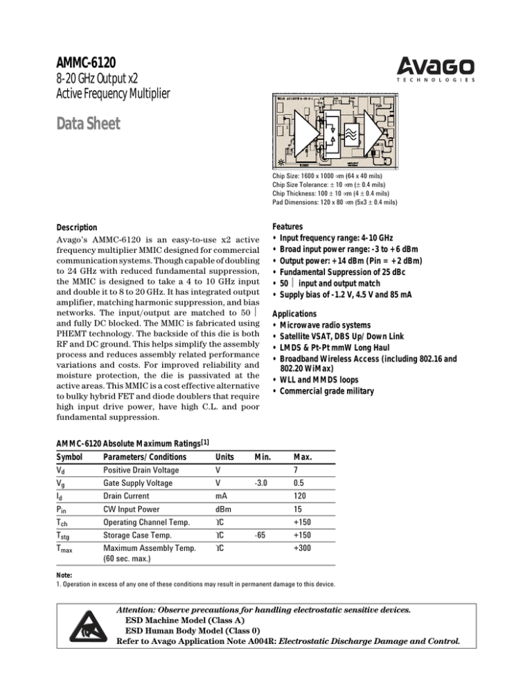
Chip Size: 1600 x 1000 µm (64 x 40 mils)
Chip Size Tolerance: ± 10 µm (± 0.4 mils)
Chip Thickness: 100 ± 10 µm (4 ± 0.4 mils)
Pad Dimensions: 120 x 80 µm (5x3 ± 0.4 mils)
Description
Avago’s AMMC-6120 is an easy-to-use x2 active
frequency multiplier MMIC designed for commercial
communication systems. Though capable of doubling
to 24 GHz with reduced fundamental suppression,
the MMIC is designed to take a 4 to 10 GHz input
and double it to 8 to 20 GHz. It has integrated output
amplifier, matching harmonic suppression, and bias
networks. The input/output are matched to 50 Ω
and fully DC blocked. The MMIC is fabricated using
PHEMT technology. The backside of this die is both
RF and DC ground. This helps simplify the assembly
process and reduces assembly related performance
variations and costs. For improved reliability and
moisture protection, the die is passivated at the
active areas. This MMIC is a cost effective alternative
to bulky hybrid FET and diode doublers that require
high input drive power, have high C.L. and poor
fundamental suppression.
AMMC-6120 Absolute Maximum Ratings[1]
Symbol
Parameters/Conditions
Vd
Positive Drain Voltage
Vg
Gate Supply Voltage
Id
Drain Current
Pin
CW Input Power
Tch
Operating Channel Temp.
Tstg
Storage Case Temp.
Tmax
Maximum Assembly Temp.
(60 sec. max.)
Units
V
V
mA
dBm
°C
°C
°C
Min.
-3.0
-65
Features
• Input frequency range: 4-10 GHz
• Broad input power range: -3 to +6 dBm
• Output power: +14 dBm (Pin = +2 dBm)
• Fundamental Suppression of 25 dBc
• 50 Ω input and output match
• Supply bias of -1.2 V, 4.5 V and 85 mA
Applications
• Microwave radio systems
• Satellite VSAT, DBS Up/Down Link
• LMDS & Pt-Pt mmW Long Haul
• Broadband Wireless Access (including 802.16 and
802.20 WiMax)
• WLL and MMDS loops
• Commercial grade military
Max.
7
0.5
120
15
+150
+150
+300
Note:
1. Operation in excess of any one of these conditions may result in permanent damage to this device.
Attention: Observe precautions for handling electrostatic sensitive devices.
ESD Machine Model (Class A)
ESD Human Body Model (Class 0)
Refer to Avago Application Note A004R: Electrostatic Discharge Damage and Control.
AMMC-6120 DC Specifications/Physical Properties[1]
Symbol
Id
Parameters and Test Conditions
Drain Supply Current (under any
RF power drive and temperature)
(Vd = 4.5 V)
Units
mA
Min.
80
Typ.
85
Max.
105
Vg
qch-b
Gate Supply Operating Voltage
Thermal Resistance[2]
(Backside Temperature, Tb = 25°C)
V
-1.5
-1.2
-1.0
°C/W
25
Notes:
1. Ambient operational temperature TA = 25°C unless otherwise noted.
2. Channel-to-backside Thermal Resistance (qch-b) = 26°C/W at Tchannel (Tc) = 34°C as measured using infrared microscopy. Thermal Resistance at
backside temperature (Tb) = 25°C calculated from measured data.
AMMC-6120 RF Specifications [3,4,5]
TA = 25°C, Vd = 4.5 V, Id(Q) = 85 mA, Zo = 50 Ω
Symbol Parameters and Test Conditions
Units
Minimum
Typical
Fin
Input Frequency
GHz
4 to 10
Fout
Output Frequency
GHz
8 to 20
Maximum
Sigma
Po
Output
Power[4]
dBm
10.5
14
0.6
Fo
Fundamental Isolation
(referenced to Po)
dBc
18
25
1.8
3Fo
3rd Harmonic Isolation
(referenced to Po)
dBc
25
2.5
P-1dB
Input Power at 1dB Gain Compression
dBm
+1
dB
-15
dB
-9
DBc/Hz
-135
RLin
Input Return
Loss[6]
Loss[6]
RLout
Output Return
SSB
Single Sideband Phase Noise
(100 KHz offset)
Notes:
3. Small/Large -signal data measured in wafer form TA = 25°C.
4. 100% on-wafer RF test is done at Pin = +2 dBm, output frequency = 9, 16, and 20 GHz.
5. Specifications are derived from measurements in a 50-W test environment. Aspects of the multiplier performance may be improved over a more
narrow bandwidth by application of additional matching.
Typical Distribution of Pout, 2nd-Harmonic & 3rd-Harmonic Suppression (Fin = 10 GHz, Pin = 0 dBm). Based on 1800
parts sampled over several production lots.
13
14
2Fo Pout (dBm) @ 20-GHz
2
15
19
21
23
25
27
29
31
33
Fo-Suppression (dBc) @ 10-GHz
35
20
30
3Fo-Suppression(dBc) @ 30-GHz
AMMC-6120 Typical Performances (TA = 25°C, Vd = 4.5 V, ID = 85 mA, Vg = -1.2 V, Zin = Zout = 50 W unless otherwise stated)
Note: These measurements are in 50 W test environment. Aspects of the amplifier performance may be improved over a narrower bandwidth by
application of additional conjugate, linearity or low noise (Gopt) matching.
INPUT
20
16
15
15
O/P FREQ. = 2*FIN
FUNDAMENTAL
3H
4H
0
13
-5
-10
-15
12
11
10
Pin = 0
Pin = +2
Pin = +4
Pin = +6
9
-20
8
-25
7
8
10
12
14
16
18
20
22
6
24
8
10
OUTPUT FREQUENCY (GHz)
16
18
20
-20
22
-30
24
10
10
10
0
0
0
Pout (dBm)
20
-10
-20
-30
2H = 10 GHz
3H
4H
FUNDAMENTAL
-40
-11 -9 -7 -5 -3 -1 1
3
5
7
9 11
-30
-40
-11 -9 -7 -5 -3 -1 1
3
-40
-11 -9 -7 -5 -3 -1 1
5
7
9 11
20
15
15
10
10
10
5
5
5
-25
-30
-35
8
10
12
14
16
18
20
0
Pout (dBm)
Pout (dBm)
-20
-5
-10
-15
2H (@Vd = 4.0 V)
2H (@Vd = 4.5 V)
2H (@Vd = 5.0 V)
1H (@Vd = 4.0 V)
1H (@Vd = 4.5 V)
1H (@Vd = 5.0 V)
-20
-25
-30
22
24
OUTPUT FREQUENCY (GHz)
Figure 7. Typical output power and
fundamental suppression vs. temperature.
-35
26
8
10
12
14
16
18
2H = 22 GHz
3H
4H
FUNDAMENTAL
3
5
7
9 11
Figure 6. Typical output power against
fundamental, 3rd, and 4th harmonic
suppression vs. Pin (2H = 22 GHz).
20
2H (@ -40°C)
2H (@ +25°C)
2H (@ +85°C)
1H (@ -40°C)
1H (@ +25°C)
1H (@ +85°C)
22
Pin (dBm)
15
-15
18
-30
20
-10
14
-20
Figure 5. Typical output power against
fundamental, 3rd, and 4th harmonic
suppression vs. Pin (2H = 12 GHz).
0
10
-10
Pin (dBm)
-5
6
2H = 12 GHz
3H
4H
FUNDAMENTAL
Pin (dBm)
Figure 4. Typical output power against
fundamental, 3rd, and 4th harmonic
suppression vs. Pin (2H = 10 GHz).
2
Figure 3. Typical input and output return loss.
20
-10
S11
S22
FREQUENCY (GHz)
20
-20
Pout (dBm)
14
-15
-25
Figure 2. Typical output power at different
fundamental input power vs. frequency.
Pout (dBm)
Pout (dBm)
12
dBm
dBm
dBm
dBm
-10
OUTPUT FREQUENCY (GHz)
Figure 1. Typical output power against
fundamental, 3rd, and 4th harmonic
suppression (Pin = +2 dBm) vs. frequency.
3
S11 & S22 (dB)
Pout (dBm)
5
-5
14
Pout (dBm)
10
-30
OUTPUT
0
20
OUTPUT FREQUENCY (GHz)
Figure 8. Typical output power and
fundamental suppresion vs. Vd.
0
-5
2H (@Vg = -1.0 V)
2H (@Vg = -1.2 V)
2H (@Vg = -1.4 V)
1H (@Vg = -1.0 V)
1H (@Vg = -1.2 V)
1H (@Vg = -1.4 V)
-10
-15
-20
22
24
-25
-30
-11 -9 -7 -5 -3 -1 1
3
5
7
Pin (dBm)
Figure 9. Typical Pout and fundamental
suppression vs. Vg (Fout = 16 GHz).
9 11
Biasing and Operation
M/N
@ fo
should be free of any residue that
may jeopardize electrical or
mechanical attachment.
S
M/N
@ 2fo
A. DIFF. AMP
ACTIVE BALUN
The frequency doubler MMIC
consists of a differential amplifier
circuit that acts as an active balun.
The outputs of this balun feed the
gates of balanced FETs and the
drains are connected to form the
single-ended output. This results
in the fundamental frequency and
odd harmonics canceling and the
even harmonic drain currents (in
phase) adding in superposition.
Node ‘S’ acts as a virtual ground.
An input matching network (M/N)
is designed to provide good match
at fundamental frequencies and
produces high impedance
mismatch at higher harmonics.
AMMC-6120 is biased with a single
positive drain supply and single
negative gate supply using
separate bypass capacitors. It is
normally biased with the drain
supply connected to both the
VdAB and the Vdd bond pads and
the gate supply connected to the
VgD bond pad. It is important to
bypass both VdAB and Vdd with
100 pF capacitors placed as close
to the die as possible. Typical bias
connections are shown in Figure
12. For most of the application it is
recommended to use a Vg = –1.2 V
and Vd = 4.5 V.
The AMMC-6120 performance
changes very slightly with Drain
(Vd) and Gate bias (Vg) as shown
in Figure 8 and 9. Minor improvements in performance are possible
for output power or fundamental
suppression by optimizing the Vg
from –1.0 V to –1.4 V and/or Vd
from 4.0 to 5.0 V.
4
The RF input and output port are
AC coupled thus no DC voltage is
present at either ports. However,
the RF output port has a internal
output-matching circuit that
presents a DC short. Proper care
should be taken while biasing
sequential circuit to AMMC-6120
as it might cause DC short (use a
DC block if sub sequential circuit
is not AC coupled). No ground
wires are needed since ground
connections are made with plated
through-holes to the backside of
the device.
Refer the Absolute Maximum
Ratings table for allowed DC and
thermal conditions.
Assembly Techniques
The backside of the MMIC chip is
RF ground. For microstrip
applications the chip should be
attached directly to the ground
plane (e.g. circuit carrier or
heatsink) using electrically
conductive epoxy[1].
For best performance, the topside
of the MMIC should be brought up
to the same height as the circuit
surrounding it. This can be
accomplished by mounting a gold
plate metal shim (same length and
width as the MMIC) under the
chip which is of correct thickness
to make the chip and adjacent
circuit the same height. The
amount of epoxy used for the chip
and/or shim attachment should be
just enough to provide a thin fillet
around the bottom perimeter of
the chip or shim. The ground plan
The location of the RF bond pads
is shown in Figure 11. Note that all
the RF input and output ports are
in a Ground-Signal-Ground
configuration.
RF connections should be kept as
short as reasonable to minimize
performance degradation due to
undesirable series inductance. A
single bond wire is normally
sufficient for signal connections,
however double bonding with 0.7
mil gold wire or use of gold
mesh[2] is recommended for best
performance, especially near the
high end of the frequency band.
Thermosonic wedge bonding is the
preferred method for wire
attachment to the bond pads. Gold
mesh can be attached using a 2 mil
round tracking tool and a tool
force of approximately 22 grams
and a ultrasonic power of roughly
55 dB for a duration of 76 ± 8 mS.
The guided wedge at an ultrasonic
power level of 64 dB can be used
for 0.7 mil wire. The
recommended wire bond stage
temperature is 150 ± 2°C.
Caution should be taken to not
exceed the Absolute Maximum
Rating for assembly temperature
and time.
The chip is 100 µm thick and
should be handled with care. This
MMIC has exposed air bridges on
the top surface and should be
handled by the edges or with a
custom collet (do not pick up the
die with a vacuum on die center).
This MMIC is also static sensitive
and ESD precautions should be
taken.
Notes:
1. Ablebond 84-1 LM1 silver epoxy is
recommended.
2. Buckbee-Mears Corporation, St. Paul,
MN, 800-262-3824
VdAB
VgD
Vdd
RFin
RFout
Figure 10. AMMC-6120 simplified schematic.
1000
715
1310
VgD
VdAB
1478
Vdd
0
660
660
RFin
RFI
RFout
472
0
0
1600
Figure 11. AMMC-6120 bonding pad locations.
Vd
Vg
/100 pF
VdAB
/100 pF
VgD
Vdd
RFin
RFout
50 OHM LINE
Figure 12. AMMC-6120 assembly diagram.
5
50 OHM LINE
Ordering Information:
AMMC-6120-W10 = 10 devices per tray
AMMC-6120-W50 = 50 devices per tray
For product information and a complete list of distributors, please go to our website:
www.avagotech.com
Avago, Avago Technologies, and the A logo are trademarks of Avago Technologies Limited in the United States and other countries.
Data subject to change. Copyright © 2006 Avago Technologies Limited. All rights reserved. Obsoletes 5989-3759EN
5989-3944EN June 27, 2006


![dB = 10 log10 (P2/P1) dB = 20 log10 (V2/V1). dBm = 10 log (P [mW])](http://s2.studylib.net/store/data/018029789_1-223540e33bb385779125528ba7e80596-300x300.png)
