Nano made easy.
APPLICATION NOTE
Localized I-V Characterization of Photovoltaic Solar Cells
Using Monochromatic Light
Characterization is a critical part in the research of novel
solar cells and photovoltaic (PV) materials. Because the
PV properties can be affected at small scales, such as
localized traps in the bandgap for semiconductor devices,
or variances between grains in polycrystalline PV materials,
it is important to be able to characterize these devices
locally [1]. There are many parameters used in evaluating
the characteristics of photovoltaic cells and comparing
devices (e.g. conversion efficiency, fill factor, short circuit
current, etc.) These parameters are commonly evaluated
using voltage sweeps and current measurement through
use of a semiconductor parameter analyzer. Localized
measurements can be performed using laser illumination
and scanning of the device.
In collaboration with:
L.E.S.S. SA, Lausanne, Switzerland
www.less-optics.com
Imina Technologies products in use:
•
•
•
•
miBot™ BT-11 micromanipulator
Compact stage CB-42
MultiBot MB-11
syDrive SD-10 piezoelectric controller
This application note reports on using Imina Technologies
miBot micromanipulators to carry out typical photovoltaic
characterization of solar cells. A custom apparatus is
described to bring laser light coupled in an optical fiber
above the sample surface, while electrical probes contact the
device, all three using miBots to control the movements.
Apparatus
Imina Technologies components apart, the apparatus
consists of standard commercial optomechanical modules
(Thorlabs, Inc.) and a 5 mW, 532 nm, HeNe laser (Newport
Corp.) used as a light source coupled to a 250 μm diameter
optical fiber [Figures 2 and 4].
The samples are monocrystalline silicon solar cells (SOLEXPERT group, Germany) with top surface areas of 0.015
and 3.25 cm2 and open circuit voltage (VOC) specified at
0.45 V. They are placed on a sample holder mounted on a
manual X-Y stage with 25 mm of travel.
Two miBots equipped with 1 µm tungsten electrical probes
are placed near the sample on top of the X-Y stage. The
miBots are moved over individual stages (1-Bot), providing
them the ability to translate the miBot over +/- 5 mm in each
direction and to rotate them over +/- 180° while keeping
the setup very compact.
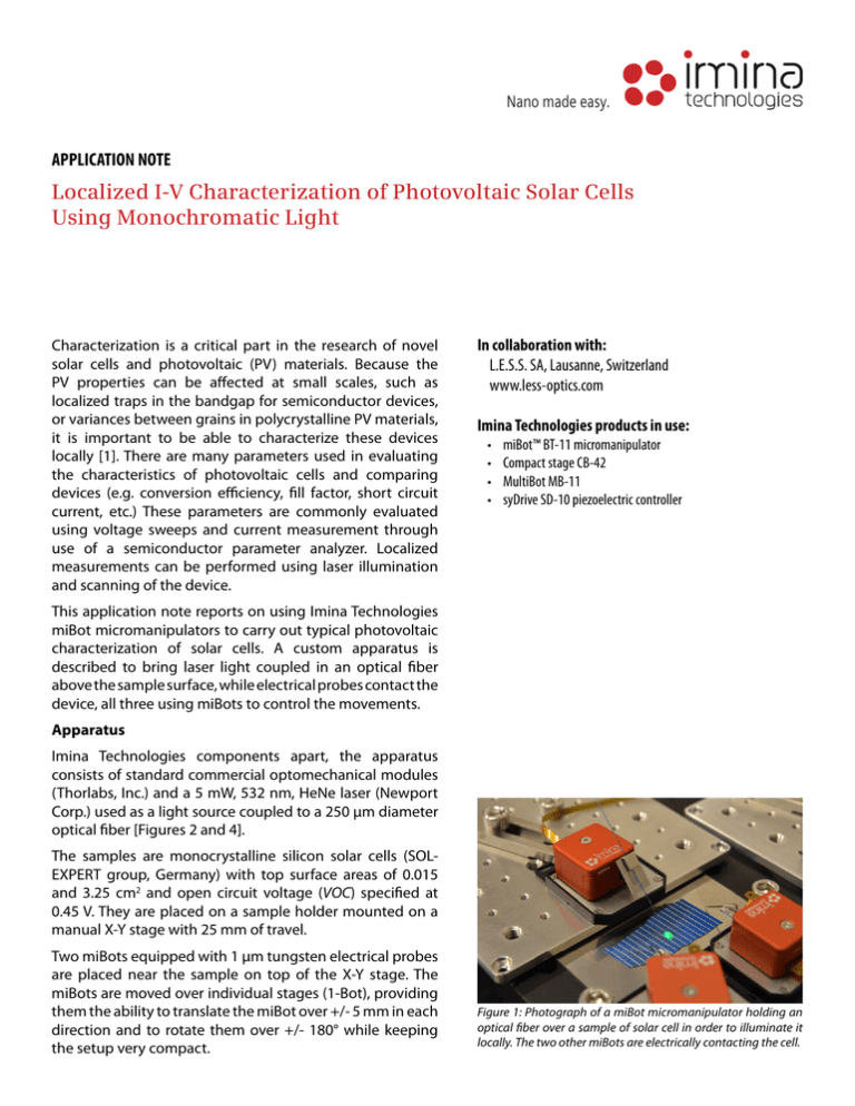
Figure 1: Photograph of a miBot micromanipulator holding an
optical fiber over a sample of solar cell in order to illuminate it
locally. The two other miBots are electrically contacting the cell.
Electrical contact is made between the negative electrode
(the thin metalized strip on the PV surface) and the positive
electrode (a conductive coating on the reverse of the
sample) through the conductive metal sample holder.
The optical fiber is positioned with a third miBot whose
1-Bot stage is fixed above the X-Y stage. The fiber is held
at 5 mm from the sample surface, making a laser spot of
approximately 2 mm in diameter [Figure 1].
Measures
Photovoltaic characteristics
The first experiment is in determining the current-voltage
characteristics of the samples using a forward bias
under illuminated conditions. These characteristics were
measured using an Agilent/HP 4156A semiconductor
parameter analyzer. First, the samples were tested with no
laser, in order to gather the photovoltaic characteristics
of the environmental lights. Then a voltage sweep of 0 to
500 mV in 2.5 mV steps was performed using the laser at
5 mW. Figure 5 and 6 illustrate the I-V curve and the power
curve produced for the 0.015 cm2 sample.
Figure 2: Schematic of the setup mounted on a standard optical
breadboard (Thorlabs).
532 nm Laser
miBot BT-11
Micromanipulators
Figure 3: Forward bias I-V curve in illuminated conditions showing PV cell parameters (Source [2]).
From the I-V curve, the short circuit current (ISC), VOC, series
resistance (Rs), and shunt resistance (Rsh) can be determined
[Figure 3]. The maximum power (Pmax) and corresponding
current (Imax) and voltage (Vmax) can be determined from the
power curve. Additionally, the solar efficiency (h) and the
field factor (FF) which give valuable information on how
a PV cell behave can be determined with the following
equations:
Device uniformity
The second experiment seeks to examine the uniformity
of the PV devices by measuring the current while the laser
Connection module
CB-42-P
MultiBot
MB-11-P
Fiber Coupler
Optical Fiber
Gradient Attenuator
Coaxial
Cables
Semiconductor Parameter
Analyzer Agilent/HP 4156A
syDrive
SD-10
USB
Computer
Control Pad
Figure 4: Block diagram and photograph of the apparatus assembly, with the sample and micromanipulators (front-right),
the syDrive piezoelectric controller and MultiBot (front-left) and
the laser followed by optical components to couple it with the
fiber (back).
spot is moved along the sample in a line. While locating
defective sites could be made possible with more advanced
techniques like LBIC, a line scan gives an idea of the
uniformity across the scan direction and one can observe
changes in the current. Figure 7 shows a line scan over the
3.25 cm2 sample linearly moved by the X-Y stage over 7 mm
in 10 seconds. In order to ensure reproducibility of the scan,
it was repeated with three passes and shifted to an average
value to account for drift in the current values between
passes. A region of visibly decreased current response
observed at the start of the scan is attributed to the fact
that the laser spot was near the edge of the sample.
Conclusions
I-V characteristics of photovoltaic samples under illuminated
conditions are successfully reported in this application note.
The positioning of the electrical probes and optical fibers
anywhere on the sample was quick thanks to the mobility
of the miBot micromanipulators over 4 degrees of freedom.
The adjustable step resolution of the piezoelectric actuators
allowed for localized illumination and measurements on
even the smallest samples. Finally, the individual miBot
stages enabled easy integration of the manipulators to the
optical setup, allowing one to take full advantage of the
compactness of the miBot and limit the footprint of the
positioning devices on the overall setup size.
Figure 5: Forward bias I-V curve for the 0.015 cm2 sample under a
5 mW laser with corresponding the ISC and VOC.
[1] S. Dueñas, E. Pérez, H. Castán, H. García, and L. Bailón, The role of defects in solar
cells: control and detection, 2013 Spanish Conference on Electron Devices (CDE), 12-14
Feb. 2013, pages 301-304. http://dx.doi.org/10.1109/CDE.2013.6481402
[2] Agilent Technologies, Inc., IV and CV Characterization of Solar/Photovoltaic Cells
Using the B1500A, Application Note B1500A-14.
Figure 6: Power curve for the 0.015 cm2 sample under a 5 mW
laser with corresponding the Pmax, Imax, Vmax, and FF.
Figure 7: Line scan over the 3.25 cm2 with three passes.
Imina Technologies SA
Quartier de l’Innovation, Bât. E
CH-1015 Lausanne
Switzerland
Phone +41 22 534 90 78
Email info@imina.ch
Web www.imina.ch
© 2013 by Imina Technologies SA. All rights reserved
