PRELIMINARY
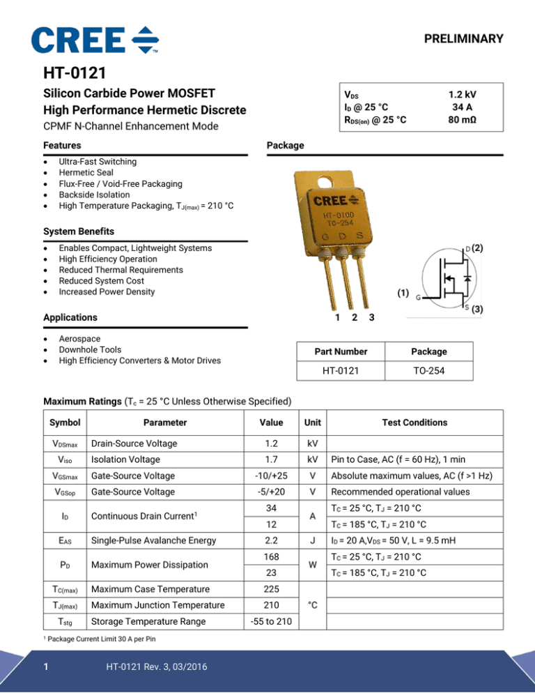
HT-0121
Silicon Carbide Power MOSFET
High Performance Hermetic Discrete
VDS
ID @ 25 °C
RDS(on) @ 25 °C
CPMF N-Channel Enhancement Mode
Features
1.2 kV
34 A
80 mΩ
Package
Ultra-Fast Switching
Hermetic Seal
Flux-Free / Void-Free Packaging
Backside Isolation
High Temperature Packaging, TJ(max) = 210 °C
System Benefits
(2)
Enables Compact, Lightweight Systems
High Efficiency Operation
Reduced Thermal Requirements
Reduced System Cost
Increased Power Density
(1)
Applications
1
Aerospace
Downhole Tools
High Efficiency Converters & Motor Drives
2
(3)
3
Part Number
Package
HT-0121
TO-254
Maximum Ratings (Tc = 25 °C Unless Otherwise Specified)
Symbol
VDSmax
Viso
Value
Unit
Drain-Source Voltage
1.2
kV
Isolation Voltage
1.7
kV
Pin to Case, AC (f = 60 Hz), 1 min
Gate-Source Voltage
-10/+25
V
Absolute maximum values, AC (f >1 Hz)
VGSop
Gate-Source Voltage
-5/+20
V
Recommended operational values
Continuous Drain Current1
34
12
EAS
Single-Pulse Avalanche Energy
PD
Maximum Power Dissipation
TC(max)
Maximum Case Temperature
225
TJ(max)
Maximum Junction Temperature
210
Tstg
Storage Temperature Range
Package Current Limit 30 A per Pin
1
Test Conditions
VGSmax
ID
1
Parameter
HT-0121 Rev. 3, 03/2016
2.2
168
23
-55 to 210
A
J
W
°C
TC = 25 °C, TJ = 210 °C
TC = 185 °C, TJ = 210 °C
ID = 20 A,VDS = 50 V, L = 9.5 mH
TC = 25 °C, TJ = 210 °C
TC = 185 °C, TJ = 210 °C
PRELIMINARY
SiC MOSFET Electrical Characterization (TC = 25 °C unless otherwise specified)
Symbol
V(BR)DSS
VGS(th)
Parameter
Drain-Source Breakdown Voltage
Gate Threshold Voltage
Min.
Typ.
Drain-Source Leakage Current
IGSS
Gate-Source Leakage Current
RDS(on)
Drain-Source On Resistance
kV
3.4
100
2.5
250
80
110
149
180
Transconductance
7.3
Ciss
Input Capacitance
1,915
Coss
Output Capacitance
120
Crss
Reverse Transfer Capacitance
13
td(on)
Turn-On Delay Time
17.2
Rise Time
13.6
td(off)
Turn-Off Delay Time
V
2.2
gfs
trv
Unit
1.2
1
IDSS
Max.
tfv
Fall Time
35.6
Eon
Turn-On Switching Loss
530
Eoff
Turn-Off Switching Loss
320
RG
Qgs
Internal Gate Resistance
Gate To Source Charge
5
23.8
Qgd
Gate To Drain Charge
43.1
Qg
Gate Charge Total
90.8
VGS = 0 V, ID = 100 μA
VDS = VGS, ID = 10 mA
VDS = 10 V, ID = 10 mA , TJ=210 C
μA
VGS = 0 V, VDS = 1200 V
VGS = 0 V, VDS=1200 V,
TJ=210 C
nA
VGS = 20 V, VDS = 0 V
mΩ
VGS = 20 V, ID = 20 A
VGS = 20 V, ID = 20 A, TJ = 210 C
S
VGS = 20 V, ID = 20 A
pF
VGS = 0 V, VDS = 800 V
f = 1 MHz, VAC = 25 mV
ns
62
Test Conditions
VDS = 800 V, VGS = -2 / +20 V
ID = 20 A
RG(ext) = 6.8 Ω, L = 856 μH
Per JEDEC24 p. 27
μJ
Ω
VGS = 0 V, f = 1 MHz, VAC= 25 mV
nC
VDS = 800 V, VGS = 0 / +20 V
ID = 20 A
Per JEDEC24 p. 27
Body Diode Electrical Characteristics (Tc = 25 °C Unless Otherwise Specified)
Symbol
2
Parameter
Value
3.3
Unit
VSD
Diode Forward Voltage
trr
Reverse Recovery Time
220
ns
Qrr
Reverse Recovery Charge
142
nC
Irrm
Peak Reverse Recovery Current
2.3
A
HT-0121 Rev. 3, 03/2016
3.1
V
Test Conditions
VGS = -5 V, ID = 10 A
VGS = -2 V, ID = 10 A
VGS = -5 V, IF = 20 A, VR = 800 V
diF/dt = 100 A/μs
PRELIMINARY
Thermal & Mechanical Characteristics
Symbol
Parameter
RΘ(J-C)
FET Thermal Resistance, J to C
W
Weight
MS
Mounting Torque
Value
Unit
1.1
°C/W
9
g
0.8
N-m
Test Conditions
6-32 Bolts
Typical Performance
100.0
200
180
160
140
120
100
80
60
40
20
0
Drain Current, ID (A)
Power Dissipation, Ptot (W)
TJ = 210 °C
tp ≤ 1 µs
10.0
tp ≤ 1 ms
1.0
DC
Tc = 25 °C
0.1
1
-50
0
50
100
150
Case Temperature, TC (°C)
200
10
100
1000
Drain Source Voltage, VDS (V)
250
Fig 2. Maximum Safe Operating Area
Fig 1. Maximum Power Dissipation Versus Case
Temperature
50
50
tp < 100 μs
45
VGS = 20 V
Drain Current, ID (A)
40
Drain Current, ID (A)
40
35
tp < 100 μs
35
30
30
25
25
VGS = 12 V
20
20
15
15
10
VGS = 8 V
10
VGS = 4 V
VGS = 8 V
5
5
0
VGS = 4 V
0
0
2
4
6
8
10
12
14
16
18
Drain to Source Voltage, VDS (V)
Fig 3. Forward Output Characteristics TJ = 25 C
3
VGS = 20 V
VGS = 16 V
VGS = 12 V
45
VGS = 16 V
HT-0121 Rev. 3, 03/2016
20
0
2
4
6
8
10
12
14
16
18
Drain-Source Voltage, VDS (V)
Fig 4. Forward Output Characteristics TJ = 210 C
20
PRELIMINARY
1.8E-1
On-Resistance (Ω)
Max. Drain Current, IDS (A)
30
TJ = 210 °C
25
20
15
1.4E-1
1.2E-1
1.0E-1
8.0E-2
25 °C
10
VGS = 20 V
6.0E-2
5
4.0E-2
0
0
-50
0
50
100
150
Case Temperature, TC (°C)
200
25 °C
75 °C
150 °C
Drain Current (A)
70
60
VDS = 20V
40
30
20
10
0
5
10
15
Gate Voltage, VGS (V)
Gate Threshold voltege, VTh (V)
Gate Voltage, VGS (V)
15
10
5
0
-5
0
25
50
75
Gate Charge, QG (nC)
Fig 9. Gate Charge Characteristics
HT-0121 Rev. 3, 03/2016
-50
0
50
100
150
Junction Temperature, Tj (°C)
200
Fig 8. Normalized Drain-Source Breakdown Voltage Versus
Junction Temperature
VDS = 800 V, IDS = 20 A
20
40
1.14
1.12
1.10
1.08
1.06
1.04
1.02
1.00
0.98
0.96
0.94
20
Fig 7. Transconductance Versus Junction
Temperature
25
30
Fig 6. On-Resistance Versus Drain Current
50
0
20
Drain Current, ID (A)
Norm. BD Voltage (pu)
80
10
250
Fig 5. Drain Current Derating Versus Case
Temperature
4
210 °C
175 °C
150 °C
1.6E-1
35
100
3.5
IDS = 1 mA
3
2.5
2
1.5
1
0.5
0
-50
0
50
100
150
200
Junction Temperature, Tj (°C)
Fig 10. Gate-Source Threshold Voltage Versus Junction
Temperature
PRELIMINARY
Package Dimensions [in(mm)]
Fig. 11 Dimensions
5
HT-0121 Rev. 3, 03/2016
PRELIMINARY
Important Notes
Some values were obtained from the CPMF-1200-S080B Rev. A device datasheet.
THE PRODUCT DESCRIBED IS AN ENGINEERING SAMPLE THAT IS NOT INTENDED FOR PRODUCTIVE USE,
IS CURRENTLY AVAILABLE FOR EVALUATION AND TESTING PURPOSES ONLY, AND IS PROVIDED “AS IS”
WITHOUT WARRANTY OF ANY KIND, INCLUDING BUT NOT LIMITED TO ANY WARRANTY OF NONINFRINGEMENT, MERCHANTABILITY, OR FITNESS FOR PARTICULAR PURPOSE. Suitability of this product for
any application may depend on product parameters not specified this document. The buyer is solely responsible for
determining such additional product details.
The data and information contained in this document is preliminary and is subject to change due to further product
evaluation and testing and/or product modifications. Accordingly, buyers are cautioned to evaluate actual products
against their needs and not to rely solely on the data and information presented in this document.
The product described has not been designed or tested for use in, and is not intended for use in, applications implanted
into the human body or in applications in which failure of the product could lead to death, personal injury or property
damage, including but not limited to equipment used in the operation of nuclear facilities, life-support machines, cardiac
defibrillators or similar emergency medical equipment, vehicle navigation, communication or control systems, or air
traffic control systems.
The product described is not eligible for Distributor Stock Rotation or Inventory Price Protection.
Copyright © 2013 - 2016 Cree Fayetteville, Inc. All rights reserved.
The information in this document is subject to change without notice.
Cree®, and Zero Recovery® are registered trademarks and the Cree logo is a
trademark
of Cree,
Inc.Rev. 3, 03/2016
6
HT-0121
For Purchasing: Email HighPerformanceSales@cree.com
Cree Fayetteville, Inc.
535 W Research Center Blvd
Fayetteville, AR 72701
USA Tel: +1.479.443.5759
www.apei.net
