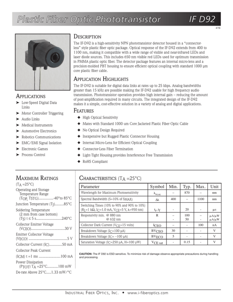
Parameter Symbol Min. Typ. Max. Unit
advertisement

4/16 Description The IF-D92 is a high-sensitivity NPN phototransistor detector housed in a “connectorless” style plastic fiber optic package. Optical response of the IF-D92 extends from 400 to 1100 nm, making it compatible with a wide range of visible and near-infrared LEDs and laser diode sources. This includes 650 nm visible red LEDs used for optimum transmission in PMMA plastic optic fiber. The detector package features an internal micro-lens and a precision-molded PBT housing to ensure efficient optical coupling with standard 1000 μm core plastic fiber cable. Application Highlights The IF-D92 is suitable for digital data links at rates up to 25 kbps. Analog bandwidths greater than 15 kHz are possible making the IF-D92 usable for high frequency audio transmission. Phototransistor operation provides high internal gain – reducing the amount of post-amplification required in many circuits. The integrated design of the IF-D92 makes it a simple, cost-effective solution in a variety of analog and digital applications. Applications ➤Low-Speed Digital Data Links Features ➤Motor Controller Triggering ➤Audio Links ◆ High Optical Sensitivity ➤Medical Instruments ◆ Mates with Standard 1000 um Core Jacketed Plastic Fiber Optic Cable ➤Automotive Electronics ◆ No Optical Design Required ➤Robotics Communications ◆ Inexpensive but Rugged Plastic Connector Housing ➤EMC/EMI Signal Isolation ◆ Internal Micro-Lens for Efficient Optical Coupling ➤Electronic Games ◆ Connector-Less Fiber Termination ➤Process Control ◆ Light-Tight Housing provides Interference Free Transmission ◆ RoHS Compliant Maximum Ratings (TA =25°C) Operating and Storage Temperature Range (TOP, TSTG)...............-40°to 85°C Junction Temperature (TJ).........85°C Soldering Temperature (2 mm from case bottom) (TS) t ≤ 5 s..........................240°C Collector Emitter Voltage (VCEO)..................................30 V Emitter Collector Voltage (VECO) .......................................5 V Collector Current (IC).............50 mA Collector Peak Current (ICM) t =1 ms ......................100 mA Power Dissipation (PTOT) TA =25°C...........100 mW De-rate Above 25°C.....1.33 mW/°C Characteristics (TA =25°C) Parameter Wavelength for Maximum Photosensitivity Spectral Bandwidth (S=10% of SMAX) Switching Times (10% to 90% and 90% to 10%) (RL=1 kΩ, IC=1.0 mA, VCE=5 V, λ=950 nm) Responsivity min. @ 880 nm @ 632 nm Collector Dark Current (VCE=15 volts) Breakdown Voltage (IC=100 μA) Breakdown Voltage (IC= –100 μA) Saturation Voltage (IC=250 μA, H=100 μW) Symbol λPEAK ∆λ tr, tf R Min. Typ. Max. Unit 400 – 1100 nm - μs – - 870 20 – - 100 50 BVCEO 30 - VCE sat - ICEO BVECO – 5 – nm – - μA/μW μA/μW - V - 100 nA - - V 0.15 - V CAUTION: The IF D92 is ESD sensitive. To minimize risk of damage observe appropriate precautions during handling and processing. I ndustrial F iber O ptics , I nc . • www.i-fiberoptics.com Relative spectral response Detector Figure 1. Typical detector response versus wavelength. Figure 3. Cross-section of fiber optic device. Fiber Termination Instructions 1.Cut off the ends of the optical fiber with a singleedge razor blade or sharp knife. Try to obtain a precise 90-degree angle (square). 2.Insert the fiber through the locking nut and into the connector until the core tip seats against the internal micro-lens. mA 3.Screw the connector locking nut down to a snug fit, locking the fiber in place. Figure 2. Rise and fall times of phototransistor. MIN 9.0 PACKAGE IDENTIFICATION: 6.86 7.11 Black housing w/ white dot • PIN 1. Emitter • PIN 2. Collector Figure 4. Case outline. Specifications are believed to be accurate but are subject to change. Industrial Fiber Optics assumes no responsibility for the consequences of using the information provided beyond replacement warranty for products not meeting stated specifications. Industrial Fiber Optics products are not authorized for use in life support applications without written approval from the President of Industrial Fiber Optics Corporation. CAUTION: • To avoid degraded device life due to package stress, do not bend or form leads outside the orientation shown on drawing. • Ensure that solder flux does not migrate into the device and block the optical path, degrading the performance. • If washing the device, liquid may become trapped in the part cavity. Ensure that all potentially corrosive materials are flushed out of the device. I ndustrial F iber O ptics , I nc . • www.i-fiberoptics.com MIN .35 .270 .280


