High Speed Carrier Injection - Cornell Nanophotonics Group
advertisement

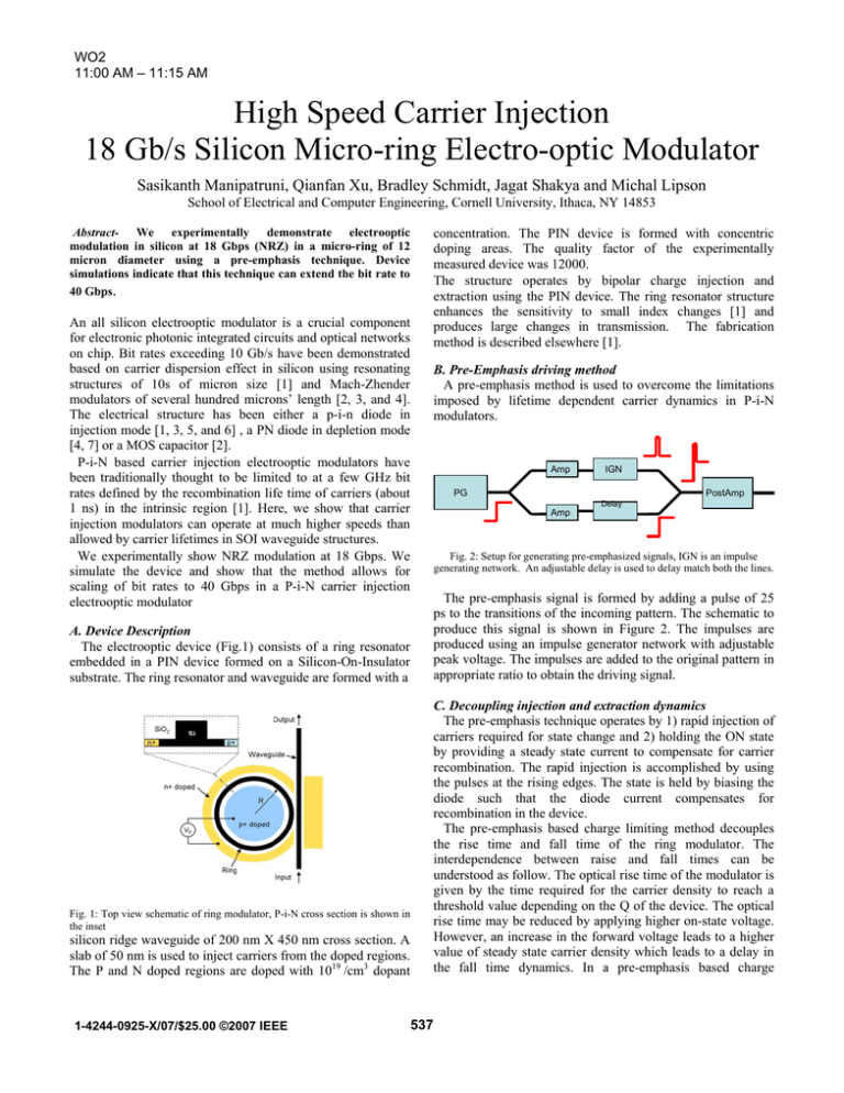
WO2 11:00 AM – 11:15 AM High Speed Carrier Injection 18 Gb/s Silicon Micro-ring Electro-optic Modulator Sasikanth Manipatruni, Qianfan Xu, Bradley Schmidt, Jagat Shakya and Michal Lipson School of Electrical and Computer Engineering, Cornell University, Ithaca, NY 14853 concentration. The PIN device is formed with concentric doping areas. The quality factor of the experimentally measured device was 12000. The structure operates by bipolar charge injection and extraction using the PIN device. The ring resonator structure enhances the sensitivity to small index changes [1] and produces large changes in transmission. The fabrication method is described elsewhere [1]. Abstract- We experimentally demonstrate electrooptic modulation in silicon at 18 Gbps (NRZ) in a micro-ring of 12 micron diameter using a pre-emphasis technique. Device simulations indicate that this technique can extend the bit rate to 40 Gbps. An all silicon electrooptic modulator is a crucial component for electronic photonic integrated circuits and optical networks on chip. Bit rates exceeding 10 Gb/s have been demonstrated based on carrier dispersion effect in silicon using resonating structures of 10s of micron size [1] and Mach-Zhender modulators of several hundred microns’ length [2, 3, and 4]. The electrical structure has been either a p-i-n diode in injection mode [1, 3, 5, and 6] , a PN diode in depletion mode [4, 7] or a MOS capacitor [2]. P-i-N based carrier injection electrooptic modulators have been traditionally thought to be limited to at a few GHz bit rates defined by the recombination life time of carriers (about 1 ns) in the intrinsic region [1]. Here, we show that carrier injection modulators can operate at much higher speeds than allowed by carrier lifetimes in SOI waveguide structures. We experimentally show NRZ modulation at 18 Gbps. We simulate the device and show that the method allows for scaling of bit rates to 40 Gbps in a P-i-N carrier injection electrooptic modulator B. Pre-Emphasis driving method A pre-emphasis method is used to overcome the limitations imposed by lifetime dependent carrier dynamics in P-i-N modulators. Amp PostAmp PG Amp Delay Fig. 2: Setup for generating pre-emphasized signals, IGN is an impulse generating network. An adjustable delay is used to delay match both the lines. The pre-emphasis signal is formed by adding a pulse of 25 ps to the transitions of the incoming pattern. The schematic to produce this signal is shown in Figure 2. The impulses are produced using an impulse generator network with adjustable peak voltage. The impulses are added to the original pattern in appropriate ratio to obtain the driving signal. A. Device Description The electrooptic device (Fig.1) consists of a ring resonator embedded in a PIN device formed on a Silicon-On-Insulator substrate. The ring resonator and waveguide are formed with a C. Decoupling injection and extraction dynamics The pre-emphasis technique operates by 1) rapid injection of carriers required for state change and 2) holding the ON state by providing a steady state current to compensate for carrier recombination. The rapid injection is accomplished by using the pulses at the rising edges. The state is held by biasing the diode such that the diode current compensates for recombination in the device. The pre-emphasis based charge limiting method decouples the rise time and fall time of the ring modulator. The interdependence between raise and fall times can be understood as follow. The optical rise time of the modulator is given by the time required for the carrier density to reach a threshold value depending on the Q of the device. The optical rise time may be reduced by applying higher on-state voltage. However, an increase in the forward voltage leads to a higher value of steady state carrier density which leads to a delay in the fall time dynamics. In a pre-emphasis based charge Fig. 1: Top view schematic of ring modulator, P-i-N cross section is shown in the inset silicon ridge waveguide of 200 nm X 450 nm cross section. A slab of 50 nm is used to inject carriers from the doped regions. The P and N doped regions are doped with 1019 /cm3 dopant 1-4244-0925-X/07/$25.00 ©2007 IEEE IGN 537 simulations a lower Q cavity would restore the extinction ratio to >10 dB still enabling 18 Gbps modulation. limiting method, the on-state carrier density is predetermined by the rising edge pulse. Hence, the the amount of charge injected is always controlled by the rising edge pulses, this leads to decoupling of rising and falling edge carrier dynamics. The pre-emphasis driving method also reduces the energy required per bit while simultaneously removing pattern dependent jitter in the modulated signal. D. Electrooptic Device Simulation We simulated the transient behavior of p-i-n embedded silicon ring device. The electrical modeling was carried out in SILVACO device simulation software. We used a contact resistance of 1 kΩ. The carrier interface recombination velocity and the surface recombination velocity are taken as 8000 cm/s each. The electron and hole lifetimes in bulk silicon are taken as 3 µs and 10 µs respectively. Modulated Signal (a.u) Fig.4 Eye diagram of 16 Gbps (NRZ) modulated optical transmission 1.6 1.2 0 0.8 0.0 200.0pS 300.0pS 800.0ps 1.6ns 2.4ns Time Fig.5 Optical transmission at 18 Gbps (NRZ) In summary, we conclude that carrier injection electrooptic modulators can work at bit rates far exceeding the limits imposed by carrier recombination dynamics by appropriate driving methods. We experimentally show 18 Gbps operation and present a method to extend the bit rate up to 40 Gbps. -4 100.0pS 0.004 0.0s -2 0.4 0.0S Applied Voltage Optical Transmission (a.u) 2 0.006 400.0pS Time Fig.3 Simulated Optical transmission at 40 Gbps (NRZ) with pre-pulsed driving signals References The optical modeling assumes the ring resonator as a unidirectional single mode traveling wave cavity coupled to waveguide with a quality factor of 8000. The fields inside the ring are calculated iteratively. The changes in refractive index and absorption of silicon are modeled via free carrier dispersion. Figure 5 shows simulated 40 Gbps transmission with >10dB extinction using pre-emphasis driving signals. Note that the transients seen at the rising edge of the optical transmission are due to the interference between the optical energy being released from the detuned cavity and the input optical energy. [1] Q. Xu, B. Schmidt, S. Pradhan, and M. Lipson, “Micrometre-scale silicon electro-optic modulator ”, Nature, Vol. 435, pp. 325-327, 19 May 2005 [2] A. Liu, R. Jones, L. Liao, D. Samara-Rubio, D. Rubin, O. Cohen, R. Nicolaescu and M. Paniccia, “A high-speed silicon optical modulator based on a metal-oxide-semiconductor capacitor,” Nature 427, 615-618 (2004). [3] F. Gan and F. X. Kärtner, "High-Speed Electrical Modulator in HighIndex-Contrast (HIC) Si-Waveguides," in Conference on Lasers and ElectroOptics, Technical Digest (CD) (Optical Society of America, 2005), paper CMG1. [4] G. Gunn, “CMOS photonicsTM - SOI learns a new trick,” in Proceedings of IEEE International SOI Conference (Institute of Electrical and Electronics Engineers, New York, 2005), pp. 7-13. [5] B. Schmidt, Q. Xu, J. Shakya, S. Manipatruni, and M. Lipson, " Compact electro-optic modulator on silicon-on-insulator substrates using cavities with ultra-small modal volumes," Opt. Express 15, 3140-3148 (2007) [6] L. Zhou and A. W. Poon, "Silicon electro-optic modulators using p-i-n diodes embedded 10-micron-diameter microdisk resonators," Opt. Express 14, 6851-6857 (2006) [7] A. Liu, L. Liao, D. Rubin, H. Nguyen, B. Ciftcioglu, Y. Chetrit, N. Izhaky, and M. Paniccia, "High-speed optical modulation based on carrier depletion in a silicon waveguide," Opt. Express 15, 660-668 (2007) [8] Q. Xu, S. Manipatruni, B. Schmidt, J. Shakya, and M. Lipson, "12.5 Gbit/s carrier-injection-based silicon micro-ring silicon modulators," Opt. Express 15, 430-436 (2007) E. Experimental results We tested the proposed scheme using a pseudo random NRZ bit sequence at 18 Gbps with +/- 2 V impulses added to an +/2V NRZ signal. The modulated bit sequence can be seen in Figure 4. In figure 5 we show the eye diagrams at 16 Gbps with extinction ratio of 8 dB. The extinction ratio at 18 Gbps is 3 dB. The degradation in extinction ratio is attributed to the long photon lifetime of the high Q cavity. As established by 538


