A new punch-through igbt having a new n -buffer layer
advertisement
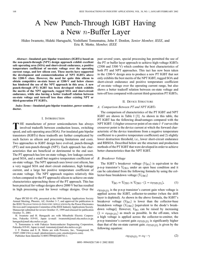
168 IEEE TRANSACTIONS ON INDUSTRY APPLICATIONS, VOL. 38, NO. 1, JANUARY/FEBRUARY 2002 A New Punch-Through IGBT Having a New n-Buffer Layer Hideo Iwamoto, Hideki Haruguchi, Yoshifumi Tomomatsu, John F. Donlon, Senior Member, IEEE, and Eric R. Motto, Member, IEEE Abstract—Insulated gate bipolar transistors (IGBTs) based on the non-punch-through (NPT) design approach exhibit excellent safe operating area (SOA) and short-circuit endurance, a positive temperature coefficient of on-state voltage over the operating current range, and low silicon cost. These merits have supported the development and commercialization of NPT IGBTs above the 1200-V class. However, the need for quite thin silicon to obtain competitive on-state losses at 1200-V and below classes has hindered the use of the NPT approach in this area. A new punch-through (PT) IGBT has been developed which exhibits the merits of the NPT approach, rugged SOA and short-circuit endurance, while also having a better tradeoff relation between on-state voltage and turn-off loss than either existing NPT or third-generation PT IGBTs. past several years, special processing has permitted the use of the PT or buffer layer approach to achieve high-voltage IGBTs (2500 and 3300 V) which combine the best characteristics of both PT and NPT approaches. This tact has now been taken in the 1200-V design area to produce a new PT IGBT that not only exhibits the best merits of the NPT IGBT, rugged SOA and short-circuit endurance and positive temperature coefficient of on-state voltage over the operating current range, but also shows a better tradeoff relation between on-state voltage and turn-off loss compared with current third-generation PT IGBTs. Index Terms—Insulated gate bipolar transistor, power semiconductor. A. Comparison Between PT and NPT IGBTs I. INTRODUCTION T HE manufacture of power semiconductors has always involved tradeoffs between conduction losses, switching speed, and safe operating area (SOA). For insulated gate bipolar transistors (IGBTs) these tradeoffs are further complicated by such factors as silicon and processing limitations and costs. Two approaches to IGBT design have evolved, punch-through (PT) and non-punch-through (NPT). Each approach has characteristics that are beneficial or detrimental to the end user. The PT approach has low on-state voltage, low leakage current, good SOA, and a small but negative temperature coefficient of on-state voltage. The NPT approach uses lower cost silicon, has a very rugged SOA and short circuit endurance, high leakage current, and a large but positive temperature coefficient of on-state voltage. The NPT approach requires relatively thin (when compared to the PT approach) silicon to achieve on-state characteristics approaching those of the PT approach. This has been practical for voltage designs above 2000 V but has resulted in high processing cost for lower voltage designs. Over the Paper IPCSD 01–076, presented at the 1999 Industry Applications Society Annual Meeting, Phoenix, AZ, October 3–7, and approved for publication in the IEEE TRANSACTIONS ON INDUSTRY APPLICATIONS by the Power Electronics Devices and Components Committee of the IEEE Industry Applications Society. Manuscript submitted for review October 15, 1999 and released for publication October 31, 2001. H. Iwamoto and H. Haruguchi are with Mitsubishi Electric Corporation, Fukuoka 819-01, Japan (e-mail: iwamotoh@mail.oka.melco.co.jp; haruguch@mail.oka.melco.co.jp). Y. Tomomatsu is with Fukuryo Semiconductor Engineering Corporation, Fukuoka 819-01, Japan (e-mail: tomomaty@mail.oka.melco.co.jp). J. F. Donlon and E. R. Motto are with Powerex, Inc., Youngwood, PA 15697-1800 USA (e-mail: jdonlon@pwrx.com; emotto@pwrx.com). Publisher Item Identifier S 0093-9994(02)00783-1. II. DEVICE STRUCTURE The comparison of characteristics of the PT IGBT and NPT IGBT are shown in Table I [3]. As shown in this table, the PT IGBT has the following disadvantages compared with the NPT IGBT: 1) higher crossover point of on-state I–V curves (the crossover point is the device current at which the forward characteristic of the device transitions from a negative temperature coefficient to a positive temperature coefficient) and 2) slightly lower destruction threshold, i.e., lower short-circuit endurance and RBSOA. Described below are the structure and production methods of the PT IGBT that were developed in order to achieve better characteristics than the NPT IGBT. B. Breakover Voltage is equivalent to the The IGBT’s breakover voltage under an open base condition and it p-n-p transistor’s can be calculated from the following formula by using the collector-base breakdown voltage (1) is the p-n-p transistor’s current gain when voltage is applied across the IGBT, collector-to-emitter (when the drift layer is depleted). As shown in the above formula, the IGBT’s is lower than the collector-base breakover voltage [equivalent to the diode’s breakbreakdown voltage can be raised by increasing down voltage]. However, as much as possible. In the off-state, when a high voltage is applied across the collector-to-emitter, the is significantly higher p-n-p transistor’s current gain is given by the than that of the on-state current gain. following equation: 0093–9994/02$17.00 © 2002 IEEE (2) IWAMOTO et al.: A NEW PT IGBT 169 TABLE I PT AND NPT IGBT CHARACTERISTICS where is the base transport factor, and efficiency. is calculated by is the Injection (3) is the drift layer width, and is the diffusion length. In buffer layer. Also, general, the NPT IGBT does not have an its injection efficiency is controlled by limiting the concentration of the collector layer and the NPT IGBT does not involve lifetime control. In order to increase the breakover voltage of an needs to be minimized by increasing the thickNPT IGBT, . On the other hand, the PT IGBT’s buffer layer ness of is short or thin. Sufficient voltage can be obtained even if the is made thin because its is low. In other words, the PT IGBT’s breakover voltage can be improved and its leakage curlayer because the rent can be reduced in spite of a thinner buffer layer. PT IGBT has an (a) C. On-State Voltage The IGBT tion [1]: can be obtained from the following equa- (4) is the voltage drop caused by the channel current of where is the forward voltage drop the MOSFET region, and collector layer, the of the diode region that consists of the buffer layer, and the drift layer. As aforementioned, the drift layer needs to be thicker than that of the NPT IGBT’s PT IGBT in order to secure its breakdown voltage because the buffer layer. This increases the NPT IGBT does not have an . Since greatly PNP transistor’s current gain , the NPT IGBT’s increases and, depends on becomes higher than that therefore, the NPT IGBT’s of the PT IGBT. Thus, the PT IGBT exhibits the advantage that its on-state voltage is lower than that of the NPT IGBT. D. Switching Characteristics A tail current is generated in the switching process when exbase cess carriers, which are stored in the p-n-p transistor’s area, disappear by their recombination. It is reported that the tail current can be calculated from the following equation [2]: (5) is the carrier lifetime of base area. This equation inwhere needs to be reduced in order to decrease dicates that the tail current and the tail time. However, the NPT IGBT’s tail (b) (c) Fig. 1. Cross-sectional views of 1200-V IGBTs. (a) PT IGBT with new buffer layer. (b) PT IGBT. (c) NPT IGBT. current is higher and its tail time is longer. This is due to the that results because the NPT IGBT has neither lifetime high buffer layer. On the other hand, the PT IGBT, control nor an buffer with the use of lifetime control, has a short lifetime and tail current are low and layer. Therefore, the PT IGBT’s its tail time is short. Additionally, the use of local lifetime redrift layer can reduce the tail time while still duction in the controlling the saturation voltage. E. Cross Point of On-State Characteristics Described below are the reasons why the NPT IGBT’s cross C and C characpoint (the point where the teristic curve of I versus V in on-state cross) is lower than that of the PT IGBT. 1) Because the built-in potential decreases as the junction temperature rises, saturation voltage in the low-current region drops as the temperature rises. 2) The inclination or slope of the I–V curve’s straight-line area is a function of mobility and lifetime. 3) Because the NPT IGBT does not use lifetime control, its lifetime value is very long and it barely affects the saturation voltage. Its I–V characteristics are, therefore, influenced by the mobility’s temperature dependency alone. The mobility drops as the temperature rises, and the inclination of the I–V curve becomes smaller as the temperature rises (i.e., on-state voltage significantly increases), and the crossover point becomes lower as a result. 170 IEEE TRANSACTIONS ON INDUSTRY APPLICATIONS, VOL. 38, NO. 1, JANUARY/FEBRUARY 2002 Fig. 4. Off-state characteristics of IGBTs whose relative impurity concentration of the n layer is 1.0 shown in Fig. 3. Fig. 2. Impurity concentration profile of new PT IGBT. Fig. 5. Electrical field distribution of new PT IGBT (simulation). V 1200 V. Fig. 3. Simulation result of 1200-V IGBTs. Case A: without n-buffer layer; case B: with n-buffer layer ( = ); case C: with n-buffer layer ( < ). 4) In the case of the standard PT IGBT, the whole IGBT is lifetime controlled by electron beam irradiation and its lifetime greatly affects the saturation voltage. The lifetime is dependent on temperature and it becomes longer as the temperature rises. Therefore, the increase in lifetime offsets the drop in mobility and the difference as a function of temperature between the I–V curve’s inclination becomes small. As a result, the crossover point rises. As seen from the above descriptions, the crossover point of the NPT IGBT is lower because of the lifetime control and not because of the structure. It means the crossover point of the PT IGBT can be lowered by reducing the lifetime control. With conventional PT IGBTs, the whole chip is treated for lifetime control by electron beam irradiation. Therefore, its crossover point can be lowered using local lifetime control [4]. = F. Ruggedness Destruction tolerance is greatly influenced by both layer thickness and . In order to secure the required layer needs to breakover voltage for an NPT IGBT, the be thicker. Consequently, the destruction tolerance becomes high. Therefore, the destruction tolerance of the PT IGBT could be increased by optimizing the thickness of the layer. However, this approach also increases the saturation voltage and switching loss. One can reduce these drawbacks by forming a local lifetime-controlled layer adjacent to the layer and optimizing the doping density in the layer. That is, it is possible to ensure high destruction tolerance without much effect on the saturation voltage and switching losses by buffer layer in which the lifetime is controlled adopting an layer. short and increasing the doping density slightly in the G. How to Realize a Superior PT IGBT The PT IGBT’s characteristics can be improved by the following. IWAMOTO et al.: A NEW PT IGBT 171 Fig. 6. Off-state characteristic of new PT IGBT. (a) With proton irradiation. (b) Without proton irradiation. (Horizontal: 200 V/div; vertical: 200 A/div.) (a) (b) and switching loss tradeoff. Measurement conditions: T = 15 V; I = 30 A; switching loss: V = 600 V; = 15 V; and I = 30 A. = Fig. 8. Forward I–V characteristics at T = 25 C and 125 C (horizontal: 500 mV/div, vertical: 5 A/div). (a) New PT IGBT (30 A). (b) Conventional PT IGBT (30 A). 1) The drift layer should be made as thin as possible in order to reduce the saturation voltage. 2) To reduce turn-off time, it is effective to reduce the lifedrift layer that is not depleted when the time of the off-state voltage is applied. 3) An -buffer layer needs to be constructed in order to secure a high breakover voltage for the IGBT that has a thin drift layer. 4) The lifetime control should be minimized in order to lower the crossover point of the on-state characteristic I–V curves. drift layer should be optimized 5) The thickness of the to improve the destruction tolerance. Fig. 1 compares schematic cross sections of the newly developed PT IGBT [Fig. 1(a)] with a conventional PT IGBT [Fig. 1(b)] and the NPT IGBT [Fig. 1(c)]. Fig. 1(a) is the new PT IGBT with the newly developed -buffer layer. A collector region is formed with an approximately 100- m boron diffused layer over an -type single layer is designed so crystal wafer. The thickness of the that the depletion layer extends to the collector region when layer rated voltage is applied at off state. That is, the is some 10- m thicker than that of the PT IGBT shown in Fig. 1(b). This -buffer layer is formed by first applying proton irradiation near the border between the collector area and layer and then it is annealed. The buffer layer having the substrate is formed by changing lower resistivity than the the proton irradiated area to a donor area. Also, the IGBT’s is controlled by changing the anneal time to control the local lifetime [5]. Fig. 2 shows the resulting measurement of the newly developed PT IGBT’s impurity concentration Fig. 7. V 125 C; V 6V :V H. New Structure for PT IGBT Based on the aforementioned analysis, an -buffer layer was constructed by newly developed methods, and a new PT IGBT drift layer thickness has been developed. with an optimized 172 IEEE TRANSACTIONS ON INDUSTRY APPLICATIONS, VOL. 38, NO. 1, JANUARY/FEBRUARY 2002 (a) (b) Fig. 9. Turn-off switching waveforms. (a) New PT IGBT. (b) Conventional PT IGBT. V (I : 5 A/div; V : 100 V/div; t: 500 ns/div). = 600 V; 6V = 15 V; T = 125 C; R = 11 ; L = 1 mH profile after annealing. This curve confirms that the resistivity drops when the proton irradiated area turns to a donor area and the -buffer layer is formed. Fig. 1(b) shows the structure of a conventional PT IGBT that uses an epitaxial wafer, and Fig. 1(c) shows the structure of a conventional NPT IGBT that uses an -type single crystal wafer of 250- m thickness. The conventional PT IGBT uses electron beam irradiation and the whole chip is lifetime controlled. The is NPT IGBT does not involve lifetime control and its maintained within an appropriate value by limiting the collector concentration. All the IGBT chips that were used for the new PT, the conventional PT, and the NPT fabricated models exA/cm ). amined for this comparison are 1200 V, 30 A ( Fig. 10. Switching waveform of new PT IGBT under the condition of short = 800 V; V = 15 V circuit. Test conditions: T = 125 C; V (V : 200 V/div; I : 50 A/div; t: 5 s/div). 6 III. DEVICE SIMULATION Breakover voltage simulation results are shown for three 1200-V designs in Fig. 3. Case A is for an IGBT without -buffer layer, Case B is for an IGBT with an -buffer layer layer, and Case C is for an having the same lifetime as the IGBT with an -buffer layer having shorter lifetime than the drift layer. The concentration of the -buffer layer comes from the value obtained from Fig. 2. The -layer thickness was kept constant (150 m) and its concentration varied. The simulation confirms that, for Case A, the breakover decreases when the impurity concentration voltage drops below 1.2. That is because the depletion layer extends to collector at low drift layer concentration. On the the other hand, for Case B, the breakover voltage increases as the impurity concentration decreases. This is because the -buffer layer prevents the depletion layer from extending to the collector. As for Case C, the breakover voltage is much higher of the p-n-p transistor, than Case B. This is because the which is composed of the IGBT’s base area, area, and collector area, decreases. Fig. 4 shows the off-state I–V characteristics of the three layer concentration of 1.0 (relative cases, A, B, and C, at an value). From these figures, it is clear that the breakover voltage drift layer concentration of Case A peaks at a particular value and Case C has the highest breakdown voltage. needs to be reduced so that a According to (1), high breakover voltage can be attained. The new IGBT with the -buffer layer that is formed by the aforementioned methods has a short lifetime and low resistance. Therefore, higher breakover drift layer is made voltage can be attained even though the thinner than that of an NPT IGBT. Shown in Fig. 5 is the electrical field distribution inside the chip when 1200 V is applied across the collector-to-emitter when the impurity concentration is 1.0 in Fig. 3 Case B. Fig. 5 shows that the electric field suddenly drops near the -buffer layer for Case B. That is, the depletion layer is blocked from reaching through the collector layer by the -buffer layer. A stable breakover voltage can be obtained even if slight variadrift layer thickness and drift layer impurity tions in concentration are observed during production. Thus, this is one of the merits of forming the -buffer layer. Simulation was also carried out to assess the temperature dependence of the on-state I–V characteristic. It was confirmed that, with the use of local lifetime control, the crossover point C and C was far below of the two I–V curves at rated current. IV. EXPERIMENTAL RESULTS A fabricated model of a PT IGBT, whose drift layer thickness is 150 m and impurity concentration in the case of Fig. 3 is 1.0, has been made and evaluated. The evaluation results are as follows. IWAMOTO et al.: A NEW PT IGBT 173 Fig. 11. Switching waveform for RBSOA test of new PT IGBT. Measurement conditions: (V : 200 V/div; I : 50 A/div; t: 500 ns/div). A. Breakover Voltage The new PT IGBT’s V–I characteristic at off-state is shown in Fig. 6. Fig. 6(b) shows the characteristics before proton irradiation (equivalent to Case A of simulation results) and Fig. 6(a) shows them after the proton irradiated area became a donor area (equivalent to Case C of the simulation.) Fig. 6(a) shows that the new PT IGBT has a sufficient breakover voltage for the 1200-V class as the result of formation of an -buffer layer and reduction of the proton irradiated area’s lifetime. Also, the simulation results shown in Fig. 4 very much agree with the measurement results shown in Fig. 6; and those figures point out the trend of the breakover voltage shift before and after the formation of the -buffer layer match. B. Tradeoff Between On-State Voltage and Switching Loss and turn-off switching loss is Tradeoff between shown in Fig. 7. Generally, the turn-off loss is defined as a loss generated at turn-off from when the collector voltage reaches 10% at its rise to when the collector current falls to 10%. However, if the turn-off loss is measured according to this definition, the turn-off losses of the new PT IGBT and NPT IGBT turn out to be understated and inaccurately compared since the current tail drags long into the area where current is low. In order to make a fair comparison against the conventional PT IGBT, the turn-off loss here is defined as the loss from when the voltage reaches 10% at its rise to when the current falls to 2%. Fig. 7 is the measurement result based on this definition. values of the chips used in the new PT IGBT are of the changed by altering the anneal time. Also, the NPT IGBT is changed by altering the boron concentration of drift layer of the new PT IGBT the collector layer. The can be made thinner than that of the NPT IGBT and, therefore, the new PT IGBT has better characteristics. Also, the new PT IGBT has better characteristics than the conventional PT IGBT drift layer. This is because the new despite it having a thicker PT IGBT uses local lifetime control with proton irradiation. C. On-State Characteristics Shown in Fig. 8 are the output characteristics of the new PT C and IGBT and the conventional PT IGBT at C. The crossover point of the new PT IGBT that uses local T = 125 C; V = 1200 V; I = 150 A; 6V = 15 V lifetime control is very low. Therefore, this IGBT has the merit that current can be easily balanced when connected in parallel. D. Switching Characteristics Fig. 9 shows the current and voltage switching waveforms of the new PT IGBT and conventional PT IGBT at load at turn-off. These waveforms show that the turn-off loss of the new PT IGBT does not increase much compared to the conventional PT IGBT because of the small increase in the tail current even though its temperature is high (125 C). This is because the new PT IGBT uses local lifetime control by proton irradiation and is little affected by lifetime temperature shift compared to the conventional PT IGBT whose whole wafer’s lifetime is controlled by electron beam irradiation. However, the new PT IGBT’s tail time is longer than that of the conventional PT IGBT because drift layer is thicker than that of the the new PT IGBT’s conventional PT IGBT. Yet, the new PT IGBT’s turn-off loss is lower since its tail current is lower and its length is shorter. E. Ruggedness Shown in Fig. 10 is the switching waveform of the new PT-IGBT under short-circuit condition. As shown here, the new PT IGBT is not damaged, even if the short-circuit duration is 20 s. Thus, it has more than sufficient short-circuit endurance for actual application use. Fig. 11 shows the switching waveform for the RBSOA test of the new PT IGBT. It was confirmed that the new PT IGBT is capable of turning off 150 A (current A/cm ) which is 5 the rated current under such density harsh conditions. Thus, the new PT IGBT has a larger turn-off capability (RBSOA) than that of the conventional PT IGBT. V. CONCLUSION Experimental results demonstrated that heat treatment (annealing) reduced the resistivity in the proton irradiated -type region of a PT IGBT. Application of this phenomenon allowed development of a 1200-V PT IGBT having a new -buffer layer. Experiments verified that the new PT IGBT has the merits of an NPT IGBT, with the crossover point of the I–V curves at C and C far below the rated current and with high short-circuit endurance. In addition, lower losses than with existing third-generation PT IGBTs were achieved. 174 IEEE TRANSACTIONS ON INDUSTRY APPLICATIONS, VOL. 38, NO. 1, JANUARY/FEBRUARY 2002 REFERENCES [1] B. J. Baliga, Modern Power Devices. Melbourne, FL: Krieger, 1992, p. 358. [2] D. S. Kuo et al., “Modeling the turn-off characteristics of bipolar MOS transistor,” IEEE Electron Device Lett., vol. EDL-6, pp. 211–214, June 1985. [3] J. Yamashita, T. Yamada, S. Uchida, H. Yamaguchi, and S. Ishizawa, “A relation between dynamic saturation characteristics and tail current of nonpunchthrough IGBT,” in Conf. Rec. IEEE-IAS Annu. Meeting, vol. 3, 1996, pp. 1425–1432. [4] K. Mochizuki, K. Ishii, M. Takeda, H. Hagino, and T. Yamada, “Examination of punch through IGBT for high voltage and high current applications,” in Proc. Int. Symp. Power Semiconductor Devices, 1997, pp. 237–240. [5] W. Wondrak and D. Silber, “Buried recombination layers with enhanced -type conductivity for silicon power devices,” Phisica BC, vol. 129, pp. 322–326, 1985. N Hideo Iwamoto was born in Japan in 1943. He received the B.E. degree in electrical engineering from Osaka University, Osaka, Japan, and the Doctor of Engineering degree from Yamaguchi University, Yamaguchi, Japan, in 1967 and 2001, respectively. He was with Mitsubishi Electric Corporation from 1967 to 1991. He was with Powerex, Inc., Youngwood, PA, from 1992 to 1998, prior to reurning to Mitsubishi Electric Corporation, Fukuoka, Japan, in 1999. He has been engaged in the design and development of power semiconductor devices. Mr. Iwamoto is a member of the Institute of Electrical Engineers of Japan. Hideki Haruguchi was born in Kagoshima Prefecture, Japan, in 1968. He received the B.S. degree in electrical engineering from Kumamoto University, Kumamoto, Japan, in 1991. Since 1991, he has been with the Engineering Development and Design Section, Power Semiconductor Division, Mitsubishi Electric Corporation, Fukuoka, Japan, where he has worked on the design of power semiconductor devices, in particular, the design of IGBT chips. Yoshifumi Tomomatsu was born in 1967. He received the B.S. degree in applied physics from Fukuoka University, Fukuoka, Japan, in 1989. In 1989, he joined Fukuryo Semiconductor Engineering Corporation, Fukuoka, Japan, a subsidiary group of Mitsubishi Electric Corporation. He is a Design and Development Engineer for power semiconductors (IGBT and diode). Mr. Tomomatsu is a member of the Institute of Electrical Engineers of Japan. John F. Donlon (S’64–M’66–SM’93) received the B.S. degree with high honors from the University of Lowell, Lowell, MA, and the M.S. degree from Syracuse University, Syracuse, NY, in 1966 and 1970, respectively, both in electrical engineering. While at Syracuse University, he studied under a National Aeronautics and Space Administration Traineeship. He is Senior Application Engineer at Powerex, Inc., Youngwood, PA, and has been involved in the rating, evaluation, and application of power semiconductors for the past 31 years. He represents Powerex on the Electronic Industries Alliance JEDEC Standards Committee for Rectifiers and Thyristors and chairs the Committee on Transistors. He has been active in the publication of application notes and technical papers describing the characteristics and proper application of power semiconductors. Mr. Donlon is a senior member of the IEEE Industry Applications Society and a member of the IEEE Power Electronics Society, Tau Epsilon Sigma, and Eta Kappa Nu. Eric R. Motto (M’90) received the B.S. degree in electrical engineering from The Pennsylvania State University, University Park, and the B.A. degree in mathematics from Saint Vincent College, Latrobe, PA, in 1987. He is a Principal Application Engineer with Powerex, Inc., Youngwood, PA, and has been involved in the evaluation and application of IGBT and intelligent power modules since 1990. He has written and presented more than 20 conference technical papers and authored numerous application notes and trade magazine articles.
