Common Mode Filter Project by Means of Internal Impedance
advertisement

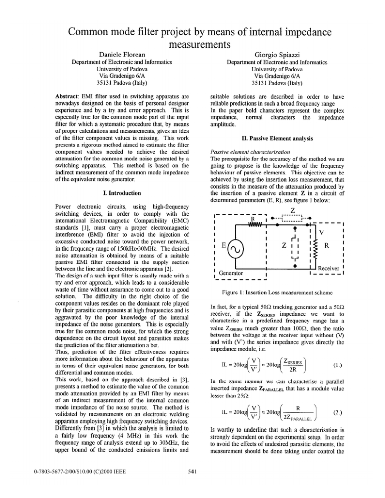
Common mode filter project by means of internal impedance measurements Daniele Florean Department of Electronic and Informatics University of Padova Via Gradenigo 6/A 35 13 1 Padova (Italy) Giorgio Spiazzi Department of Electronic and Informatics University of Padova Via Gradenigo 6/A 3 5 13 1 Padova (Italy) EM1 filter used in switching apparatus are nowadays designed on the basis of personal designer experience and by a try and error approach. This is especially true for the common mode part of the input filter for which a systematic procedure that, by means of proper calculations and measurements, gives an idea of the filter component values is missing. This work presents a rigorous method aimed to estimate the filter component values needed to achieve the desired attenuation for the common mode noise generated by a switching apparatus. This method is based on the indirect measurement of the common mode impedance of the equivalent noise generator. suitable solutions are described in order to have reliable predictions in such a broad frequency range In the paper bold characters represent the complex imped‘ance, normal characters the impedance amplitude. Abstract: I. Introduction Power electronic circuits, using high-frequency switching devices, in order to comply with the international Electromagnetic Compatibility (EMC) standards [l], must carry a proper electromagnetic interference (EMI) filter to avoid the injection of excessive conducted noise toward the power network, in the frequency range of 15OkHz-3OMHz. The desired noise attenuation is obtained by mecans of a suitable passive EM1 filter connected in the supply section between the line and the electronic app<aratus[2]. The design of a such input filter is usually made with a try and error approach, which leads to a considerable waste of time without assurance to come out to a good solution. The difficulty in the right choice of the component values resides on the dominant role played by their parasitic components at high frequencies and is aggravated by the poor knowledge of the internal imped<ance of the noise generators. This is especially true for the common mode noise, for which the strong dependence on the circuit layout ‘and parnsitics m(akes the prediction of the filter attenuation a bet. Thus, prediction of the filter effectiveness requires more information about the behaviour of the apparatus in terms of their equivalent noise generators, for both differential and common modes. This work, based on the approach described in [3], presents a method to estimate the value of the common mode attenuation provided by an EM1 filter by means of an indirect measurement of the internal common mode impedance of the noise source. The method is validated by measurements on an electronic welding apparatus employing high frequency switching devices. Differently from [3] in which the analysis is limited to a fairly low frequency (4 MHz) in this work the frequency range of analysis extend up to 3OMHz, the upper bound of the conducted emissions limits and 0-7803-5677-2/00/$10.00 (C)2000 IEEE 541 II. Passive Element analysis Passive element characterisation The prerequisite for the accuracy of the method we are going to propose is the knowledge of the frequency behaviour of passive elements. This objective can be achieved by using the insertion loss measurement, that consists in the measure of the attenuation produced by the insertion of a passive element Z in a circuit of determined parameters (E, R), see figure 1 below: 1 CenemdReceiver , ‘ j I I ----- Figure 1: Insertion Loss measurement scheme In fact, for a typical 5OQ tracking generator and a 5Ofi receiver, if the &Em, impedance we want to characterise in a predefined frequency range has a value ZsERIEsmuch greater than 100.0, then the ratio between the voltage at the receiver input without (V) and with (V’) the series impedance gives directly the impedance module, i.e. IL = 2010g($) Y 2olog(+) (1.) In the same manner we can characterise a parallel inserted impedance Zpm,,, that has a module value lesser th~an25Q IL = 201,,(+) = ZOlog( 2zrL,,) (2.) Is worthy to underline that such a characterisation is strongly dependent on the experimental setup. In order to avoid the effects of undesired p‘arasitic elements, the measurement should be done taking under control the possible sources of unidealities as the length of the connections, the proximity of ground planes and of other metallic objects, etc. As an example, the following passive components have been characterised with this method: inductors L, (3mH) and L2 (4OOuH), and capacitors C1 (47nF), C2 (220nF) and C3 (1uF) (polyester type), in the frequency range of lSOkHz-3OMHz. The appropriate insertion loss method was used, i.e. since the inductors presents at the frequencies of analysis an impedance greater than lOOohm they are characterised with the series insertion, while the capacitors, which have an impedance lower than 25ohm, are characterised with the parallel insertion. The results are shown in figure 2 for the inductors and figure 3 for the capacitors. The graph of the inductor L2 presents an angular progress due to the limited number of point, in <anycase is clear the non ideal behaviour of the component. It is interesting to observe that, due to the parasitic series inductance, the three capacitors show the same impedance above 10MHz: this means that they will give the same degree of attenuation when used as filters in the high frequency range. This happens because the series parasitic inductance due to the external connections dominates in this frequency range. lo4 Parasitic parameters identification It is possible to obtain <anequivalent electric model of such passive components by extracting the value of their parasitic parameters from the measured impedance. A valid model of a passive element up to high frequencies is useful to understand the effects when the element is introduced in complicated layout and to obtain reliable results from circuit simulations. Figure 4a shows the electric model used to represent capacitor C, in which L, and Rr, represents its series parasitic inductance and resistance respectively (the resistance connected in parallel to the capacitance C modelling the dielectric losses was not taken into account since its effect is appreciable only at very low frequencies). Figure 4b shows the effects of each parasitic element of the model: C3., represents the value of parameter C of the model which is easily identified from the low frequency asymptote of the previously characterised impedance (labelled &REX in the figure); C3-2 represents the same capacitance but taking into account the series inductance L,, whose value can be estimated from the high frequency asymptote; lastly, the resonance peak, as observed in the measured capacitor impedance, allows to identify the series parasitic resistance Rp, as shown by the impedance of the complete model labelled C3+ As can be seen the identified parasitic element values give a satisfactory approximation of the real capacitor Ohm a> 105 Hz 10’ 107 a-n11 Figure 2: measure of the high frequency impedance of inductors L, and L2 IO2 Ohm lo4 , los Hz , , , , / , / ,, , , / , , , , ,, Hz lo* lo5 b) Figure 4: a) equivalent electric model of C3; b) comparison between the measured impedance C3REAL and different approximations: C3-, only capacitance C; G2 with L, added; C3.3 whole electric model lo8 , , , , , ,,/, Figure 3 : measure of the high frequency impedance of capacitorsCl, CZ(andCs The identificationprocessis carriedout also for an inductance with a low frequency value of 2.5mH (value often used for the common mode filter). In this case, the identification process of the parasitic elements is 542 slightly more complicated to get a satisfactory model, because it is necessary to take into account non linear behaviours like the frequency variation of the choke permeability (this phenomenon is quite pronounced in high permeability magnetic materials normally used for common mode chokes). However, a simple resistauce connected in parallel to the inductance (Rs in figure 5a) well approximates the permeability variation by means of a first order function, the pole frequency being decided from the analysis of the material property in the data sheet. The other parasitic elements &ken into account are shown in figure 5a: C, models the overall winding capacitance, while RL accounts for the core losses (the winding series resistance was ignored since its effect is limited to a very low frequency range). The comparison between the measured imped(ance (LIREAL in figure) and the successive approximations is shown in figure 5b: L,J represents the ideal inductance L of the model, which is identified from the low frequency asymptote; LIe2 shows the effect of adding the parallel capacitor C,, derived from the high frequency asymptote; Llm3 con&ins the effect of R, while Lid includes also resistance RL. Note that from the electric point of view a unique resistance could be used in the model. III. Internal commode mode impedance valuation The same insertion loss measurement can now be employed for the frequency characterisation of the impedance of an equivalent noise generator. In particular, we used a high frequency electronic welding apparatus, which must comply to [4], as a noise generator and we focused the attention on the common mode noise. In fact, differently from the differential mode noise which can be easily evaluated from the measurement of the current absorbed by the apparatus, the common mode noise is strongly influenced by parasitic elements and circuit layout, aud it often represents the dominant contribution in the high frequency range of the conducted noise measurement. Theoretical approach From a theoretical point of view the measurements of the noise generator internal impedance can be made with a series insertion or with a parallel one, the accuracy of the result depending on the value of the unknown impedance respect to the measure system input impedance R. Usually the measure system is constituted of a receiver connected to a Line Impedartce Stabilisation Network (LISN), thus the input impedance for the common mode noise of such a system is the parallel of the SO Ohm resistance of the LISN and the 50 Ohm input impedance of the receiver, (the reactive part impedance is negligible at the frequency of interest). By inserting a common mode known impedance Z,, in series between the line and the apparatus (characterised by internal impedance Z,, and noise generator E,,,) as shown in figure 6, the insertion loss results: R ____. E R+Gn IL = 201og R .E R + ‘cm + Zins I =201og l+- Ohm ‘ins R+Ln (3.) I In the hypothesis of Z,,, >> R, and Z,,, >> Z,, we obtain: IL Y 201og (4.) From (4) is easy to obtain Z,,,. Noise Generator lo* It lo5 I I Illllll HZ I &IS : I Illllll ,,,, lo* Tlq b) Figure 5: a) equivalent electric model of L, ; b) comparison between the measured impedance LIREAL and different approximations: L, -, only inductance L; L1 -2 with C, added; L1 .3 and L, -4 with I& <andRL included respectively 543 LISN+Receiver . \*:.’ V R Figure 6: measurement setup for the noise generator common mode impedance Z,, by means of a series impedance insertion. some frequency intervals: in the remaining intervals a different external impedance Z,, must be used. Otherwise inserting a known impedance Zu,sin parallel between the line and the apparatus (characterised by internal impedance Z,, and noise generator E,,, the insertion loss results: R IL = 201og Measure In order to validate the proposed measurement teclmique, the internal common mode impedance Z, of a commercial high frequency electronic welding apparatus is measured. Since, in this case, the common mode noise is mainly caused by parasitic capacitances from the electronic apparatus to the metallic chassis, a higher Z,, value as compared to R is expected. Thus, the previously characterised inductor L2 was initially used as the known series imped‘ance, following the scheme of figure 6. The resulting insertion loss measurement gave an unacceptable result in the low frequency range below MHz, since the measured impedance Z,, turned out to be not too higher than the LISN input impedance (25Ohm). As suggested above, the problem was solved by adding a parallel capacitor of known impedance (C,) in order to decrease the measure system input impedance below 20hm in the whole frequency range The comparison between the measured common mode noise produced by the electronic welding apparatus with and without the series inductance is shown in figure 7. From (4) and from the knowledge of the external impedance Z,,,, Z,, is derived: the result is reported in figure 8. As can be seen from the comparison with Zms, the hypothesis the approach is based on are satisfied ahnost in the whole frequency range from 1SOkHz to 3OMHz: only around .5MHz the obtained value doesn’t respect completely the inequality Z,, << Z,,. .E R+Ln (5.1 =201% 1+* In the hypothesis of Z,, <CR and Z,, >> Zu,s we obtain: Z IL N 201og -z?Jt ‘ins 1 . (6.1 The choice between the use of a series impedance or a parallel one depends on the expected value of Zcm: if it is much higher than 25 Ohm we use the series insertion otherwise the parallel one is the preferred choice. In any case, the measurement accuracy can be verified by checking the validity of the hypothesis done. If Z,, presents a magnitude comparable with 25 Ohm then it is convenient to decrease the receiver input impedance by using a shunt capacitor whose impedance was previously measured, as shown below. Note that the hypothesis the proposed approach is based on, could not be satisfied in the whole conducted emission frequency mnge. This means that the measured unknown impedance Z,,, is reliable only in ..--.._. -,...--..-.... : i i : ....._.. .I..-. .____._. i i 1 I qt.. . .. 1 / Figure 7: common noise produced by the welding apparatus with and without the series inductance Z,, 544 60 dB Ohm I/ pred 10’ , , , , , / /,I, lo5 / / , , , I/// J32 , , , , , ,,,u IO8 0 Figure 8: calculated Z,, ‘and measured Zuls Hz Observe that while the measure of the common mode noise was made using lots of points, Z,, was computed with 10 values per decade, resulting in a so pointed graph. The reason of this lost of quality is due to a problem raised in the comparison of the two common mode noise spectra of figure 7: the peak values resulted be not always at the same frequencies, thus requiring a shifting in frequency in order to have a reliable comparison of the two situations. This behaviour is currently under analysis. TV. Attenuation prediction and verification Once the internal impedance of the noise generator is known, it is easy to predict the insertion loss produced by the insertion of a different characterised series impedance using (3), or the attenmtion produced by a more complex common mode filter. An experimental verification of the method presented is made predicting and measuring the insertion loss produced by the insertion of the common mode inductor L, in the app‘aratus previously analysed. As we seen in figure 9 the difference between the experimental results and the predicted ones, is lower than 10 dE%, also in the middle range where the necessary approximation doesn’t match entirely the hypothesis. Figure 9: predicted and measured IL In this manner it is possible to design a filter in order to have the required noised reduction when trying to improve the conducted EMI performance of an apparatus, without relying only on experience and try and error methods. V. Conclusions The presented method allows to estimate, even roughly but rigorously, the common mode input impedance of a switching electronic apparatus and to predict the insertion loss achieved by the insertion of a common mode filter, considering the high frequency behaviour of apparatus and filter with their p<arasitics. The experimenml results showed an accuracy of about 1OdB on the predicted insertion loss. This method can be helpful for simplifying the filter design procedure, reducing development time and optimising the final solution in respect of the international conducted emission limits. References [l] European Standard: EN 55014, EN 55011, EN 55022. [2] R. L. Ozenbaugh, EMIfilter design, Dekker 1996. [3] Dongbing Zhang, Dan Y. Chen, Mark J. Nave, Dan Sable, “Measurements of Noise Source Impedance of Off-line Converters,” IEEE Applied Power Electronics Conf. Proc., 1998, pp.918 - 923. [4] EN 50199, Product standard for ac arc welding equipment. 545

