s - utm encon
advertisement

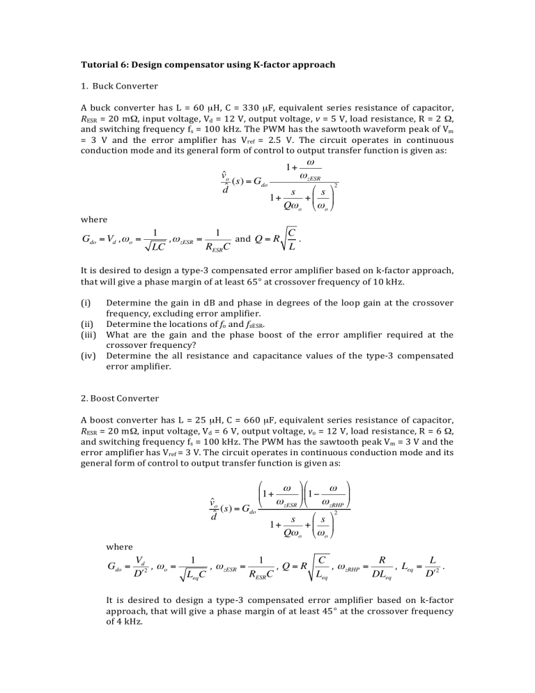
Tutorial 6: Design compensator using K-­‐factor approach 1. Buck Converter A buck converter has L = 60 µH, C = 330 µF, equivalent series resistance of capacitor, RESR = 20 mΩ, input voltage, Vd = 12 V, output voltage, v = 5 V, load resistance, R = 2 Ω, and switching frequency fs = 100 kHz. The PWM has the sawtooth waveform peak of Vm = 3 V and the error amplifier has Vref = 2.5 V. The circuit operates in continuous conduction mode and its general form of control to output transfer function is given as: ω ω zESR v̂o (s) = Gdo 2 ! s $ d̂ s 1+ +# & Qω o " ω o % 1+ where Gdo = Vd , ω o = 1 C 1 , ω zESR = and Q = R . L RESRC LC It is desired to design a type-­‐3 compensated error amplifier based on k-­‐factor approach, that will give a phase margin of at least 65° at crossover frequency of 10 kHz. (i) Determine the gain in dB and phase in degrees of the loop gain at the crossover frequency, excluding error amplifier. (ii) Determine the locations of fo and fzESR. (iii) What are the gain and the phase boost of the error amplifier required at the crossover frequency? (iv) Determine the all resistance and capacitance values of the type-­‐3 compensated error amplifier. 2. Boost Converter A boost converter has L = 25 µH, C = 660 µF, equivalent series resistance of capacitor, RESR = 20 mΩ, input voltage, Vd = 6 V, output voltage, vo = 12 V, load resistance, R = 6 Ω, and switching frequency fs = 100 kHz. The PWM has the sawtooth peak Vm = 3 V and the error amplifier has Vref = 3 V. The circuit operates in continuous conduction mode and its general form of control to output transfer function is given as: ! ω $! ω $ #1+ &#1− & v̂o " ω zESR %" ω zRHP % (s) = Gdo 2 ! s $ d̂ s 1+ +# & Qω o " ω o % where Gdo = Vd L 1 R 1 C , ω o = , ω zESR = , Q = R , ω zRHP = , Leq = 2 . 2 D! D! Leq DLeq RESRC LeqC It is desired to design a type-­‐3 compensated error amplifier based on k-­‐factor approach, that will give a phase margin of at least 45° at the crossover frequency of 4 kHz. (i) (ii) (iii) (iv) Determine the magnitude in dB and phase in degrees of the loop gain at the crossover frequency, excluding error amplifier. Determine the locations of fo, fzESR and fzRHP. What are the gain and the phase boost of the error amplifier required at the crossover frequency? Determine the all resistance and capacitance values of the type-­‐3 compensated error amplifier. 3. Buck-­‐boost Converter A buck-­‐boost converter has L = 33 µH, C = 460 µF, equivalent series resistance of capacitor, RESR = 30 mΩ, input voltage, Vd = 12 V, output voltage, |vo| = 5 V, load resistance, R = 6 Ω, and switching frequency fs = 100 kHz. The PWM has the sawtooth peak Vm = 3 V and the error amplifier has Vref = 2.5 V. The circuit operates in continuous conduction mode and its general form of control to output transfer function is given as: ! ω $! ω $ #1+ &#1− & v̂o " ω zESR %" ω zRHP % (s) = Gdo 2 ! s $ d̂ s 1+ +# & Qω o " ω o % where Gdo = Vd L 1 R 1 C , ω o = , ω zESR = , Q = R , ω zRHP = , Leq = 2 . 2 D! D! Leq DLeq RESRC LeqC It is desired to design a type-­‐3 compensated error amplifier based on k-­‐factor approach, that will give a phase margin of at least 45° at the crossover frequency of 4 kHz. (i) Determine the magnitude in dB and phase in degrees of the loop gain at the crossover frequency, excluding error amplifier. (ii) Determine the locations of fo, fzESR and fzRHP. (iii) What are the gain and the phase boost of the error amplifier required at the crossover frequency? (iv) Determine the all resistance and capacitance values of the type-­‐3 compensated error amplifier.

