DPSK-DG-10-Card 10,7Gbps
advertisement

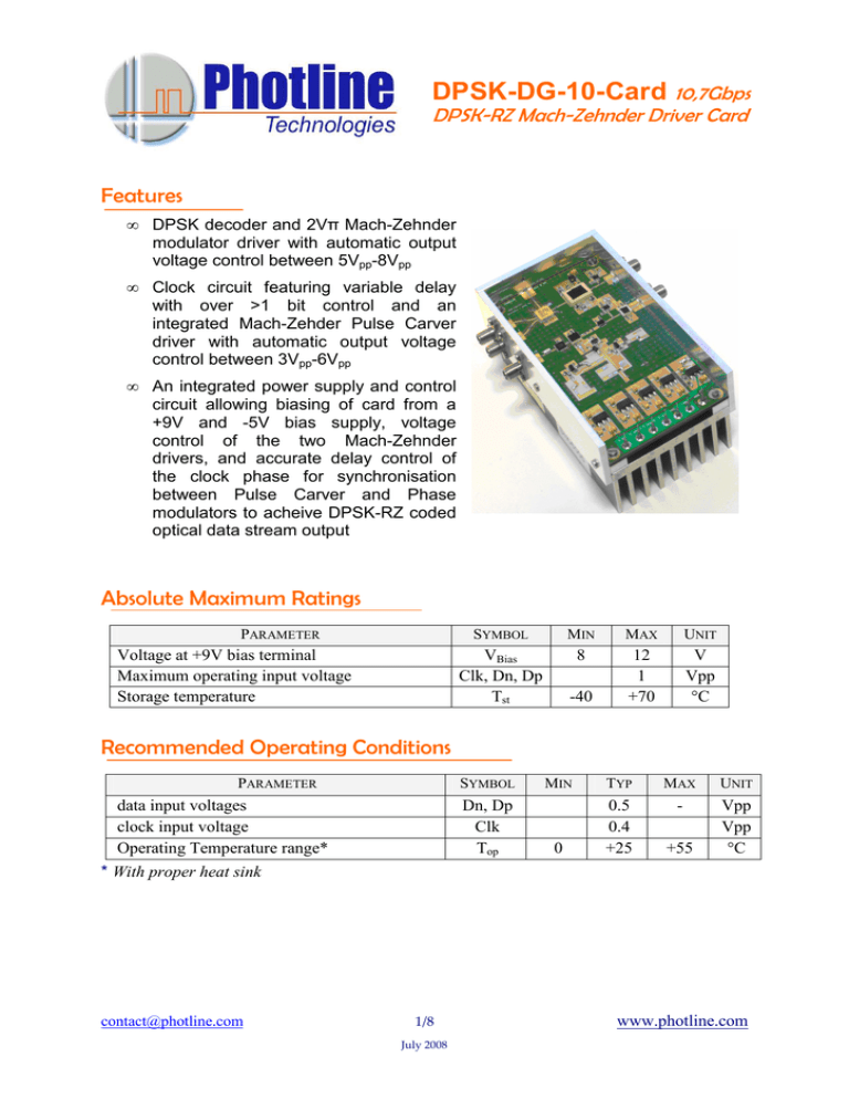
DPSK-DG-10-Card 10,7Gbps DPSK-RZ Mach-Zehnder Driver Card Features • DPSK decoder and 2Vπ Mach-Zehnder modulator driver with automatic output voltage control between 5Vpp-8Vpp • Clock circuit featuring variable delay with over >1 bit control and an integrated Mach-Zehder Pulse Carver driver with automatic output voltage control between 3Vpp-6Vpp • An integrated power supply and control circuit allowing biasing of card from a +9V and -5V bias supply, voltage control of the two Mach-Zehnder drivers, and accurate delay control of the clock phase for synchronisation between Pulse Carver and Phase modulators to acheive DPSK-RZ coded optical data stream output Absolute Maximum Ratings PARAMETER Voltage at +9V bias terminal Maximum operating input voltage Storage temperature SYMBOL MIN MAX UNIT VBias Clk, Dn, Dp Tst 8 12 1 +70 V Vpp °C -40 Recommended Operating Conditions PARAMETER SYMBOL data input voltages clock input voltage Operating Temperature range* Dn, Dp Clk Top MIN TYP MAX UNIT - 0 0.5 0.4 +25 Vpp Vpp °C +55 * With proper heat sink contact@photline.com 1/8 July 2008 www.photline.com DPSK-DG-10-Card Description 1. “Phase” section A differential pre-coder re-synchronises the input NRZ data stream and transforms it into a differential stream followed by an electro-optic modulator driver with output voltage adjustable between 5Vpp and 8Vpp. Figure 1 - Schematic of the “phase” driver section 2. “Clock” section A one bit phase adjustable circuit (>100psec) is followed by a driver, with output voltage adjustable between 3Vpp and 6Vpp, to satisfy pulse carver requirements. Figure 2 - Schematic of the clock driver section contact@photline.com 2/8 www.photline.com DPSK-DG-10-Card Electrical Characteristics Tamb = 25°C, 50 Ohm system, Vbias: +9V & -5V “Phase” Section PARAMETER Input Data rate Input Clock frequency Output Data rate Input match Data Input Match Clock Data input amplitude range Clock input amplitude range Clock Phase Margin Maximum Output Amplitude Data Output amplitude range Output amplitude eye opening Output rise/fall time Duty Cycle Range Jitter (peak-peak) Amplitude Control Voltage AGC input impedance AGC bandwidth Operating Temperature range Power dissipation Positive supply voltage Negative supply voltage Conditions Differential 50MHz-13GHz 9GHz-13GHz Differential Single-ended Single-ended Horizontal/vertical 20%-80% SYMBOL FB FCLK FB RLDin RLClkin VDin VClkin CPM VDoutmax VDout Eop tr/tf MIN 9,953 9,953 9,953 TYP 10,709 10,709 10,709 MAX 11,5 11,5 11,5 -10 -10 1200 1000 300 300 70 9 5 85 UNIT Gbps GHz Gbps dB dB mVpp mVpp ps Vpp Vpp % ps % ps V Ohm Hz °C W V V 8 45 35 55 14 5 50 Jpp VCAG 1K 3K 20 P V+ V- 55 3.2 2.5 +9 -5 “Clock” Section PARAMETER Input Clock frequency Input match Clock Output Match Clock Clock input amplitude range Clock output amplitude range Output phase delay adjustment Clock phase stability with AGC Delay control voltage Delay input impedance AGC Amplitude Control Voltage AGC input impedance Operating Temperature range Positive supply voltage Negative supply voltage Power dissipation Conditions 9,953GHz - 11,5GHz 9,953GHz - 11,5GHz Single-ended peak-peak Single-ended peak-peak SYMBOL FCLK RLin RLin VCKin VCKout Tadj MIN 9,953 Vdc 0 VCAG 0 300 3.0 100 TYP 10,709 -10 -17 MAX 11,5 -7 -12 1000 6.0 120 5 5 1000 5 1000 20 V+ VP 50 +9 -5 2.5 3.2 UNIT GHz dB dB mVpp Vpp ps ps V Ohm V Ohm °C V V W Note 1 – Depends on the stability of the amplitude of the input clock signal, bias voltages to the modules (although voltage regulators are used) and the stability of clock set voltage VampC contact@photline.com 3/8 www.photline.com DPSK-DG-10-Card Card Outline Drawing Phase Section eye diagrams (Note that the phase eye diagram is indistinguishable from an NRZ eye diagram) DOUT = 5Vpp Data rate: 10.709 Gbps 31 Ratio: ½ Pattern: 2 -1 Data amplitude NRZ_in: 0.5 Vpp Eye Amplitude : 5.02 Vpp Eye Height : 4.58 Vpp Eye Width : 85.3 ps Rise Time : 29.6 ps Fall Time : 26.9 ps Jitter RMS : 1.48 ps Jitter pp : 11.02 ps Crossing % : 50.4 % Q Factor : 33.9 V/V contact@photline.com 4/8 www.photline.com DPSK-DG-10-Card DOUT = 6.2Vpp Data rate: 10.709 Gbps 31 Ratio: ½ Pattern: 2 -1 Data amplitude NRZ_in: 0.5 Vpp Eye Amplitude: 6.20 Vpp Eye Height: 5.64 Vpp Eye Width: 84.6 ps Rise Time: 30 ps Fall Time: 27.2 ps Jitter RMS: 1.52 ps Jitter pp: 9.77 ps Crossing %: 50.3 % Q Factor: 33.65 V/V DOUT = 7.3Vpp Data rate: 10.709 Gbps 31 Ratio: ½nnnPattern: 2 -1 Data amplitude NRZ_in: 0.5 Vpp Eye Amplitude : 7.28 Vpp Eye Height : 6.63 Vpp Eye Width : 84.1 ps Rise Time : 30 ps Fall Time : 27.2 ps Jitter RMS : 1.55 ps Jitter pp : 9.89 ps Crossing % : 50.2 % Q Factor : 33.5 V/V DOUT = 8.2Vpp Data rate: 10.709 Gbps 31 Ratio: ½ Pattern: 2 -1 Data amplitude NRZ_in: 0.5 Vpp Eye Amplitude : 8.24 Vpp Eye Height : 7.24 Vpp Eye Width : 83.7 ps Rise Time : 29.5 ps Fall Time : 28.1 ps Jitter RMS : 1.67 ps Jitter pp : 10.4 ps Crossing % : 50.5 % Q Factor : 24.85 V/V contact@photline.com 5/8 www.photline.com DPSK-DG-10-Card Clock Section eye diagrams Clock output signal 3Vpp Frequency: 10.709 GHz CLK amplitude IN: 0.4 Vpp Duty Cycle: 51.8 % Rise time: 16.7 ps Fall time: 16.6 ps Clock output signal 5Vpp Frequency: 10.709 GHz CLK amplitude IN: 0.4 Vpp Duty Cycle: 49.1 % Rise time: 16.9 ps Fall time: 16.2 ps Clock output signal 6Vpp Frequency: 10.709 GHz CLK amplitude IN: 0.4 Vpp Duty Cycle: 49.1 % Rise time: 16.9 ps Fall time: 16.2 ps contact@photline.com 6/8 www.photline.com DPSK-DG-10-Card Clock Phase shift Clock Phase shift vs. Vph dc control voltage (for CLK OUT 6Vppdrive) CLK OUT=6V CLK OUT=5V CLK OUT=4V CLK OUT=3V Scale : X :18.6ps/div Y :1.21V/div Relative phase shift for different CLK OUT voltages (∆phase < 6psec) contact@photline.com 7/8 www.photline.com DPSK-DG-10-Card Photline Technologies Phone: +33 (0) 381 853 180 Fax: +33 (0) 381 811 557 16, rue Auguste Jouchoux F-25000 Besançon Photline Technologies reserves the right to change, at any time and without notice, the specifications, design, function or form of its products described herein. All statements, specification, technical information related to the products herein are given in good faith and based upon information believed to be reliable and accurate at the moment of printing. However the accuracy and completeness thereof is not guaranteed. No liability is assumed for any inaccuracies and as a result of use of the products. The user must validate all parameters for each application before use and he assumes all risks in connection with the use of the products. contact@photline.com 8/8 www.photline.com


