6F-4 50-kHz Capacitive Micromachined Ultrasonic Transducers for
advertisement

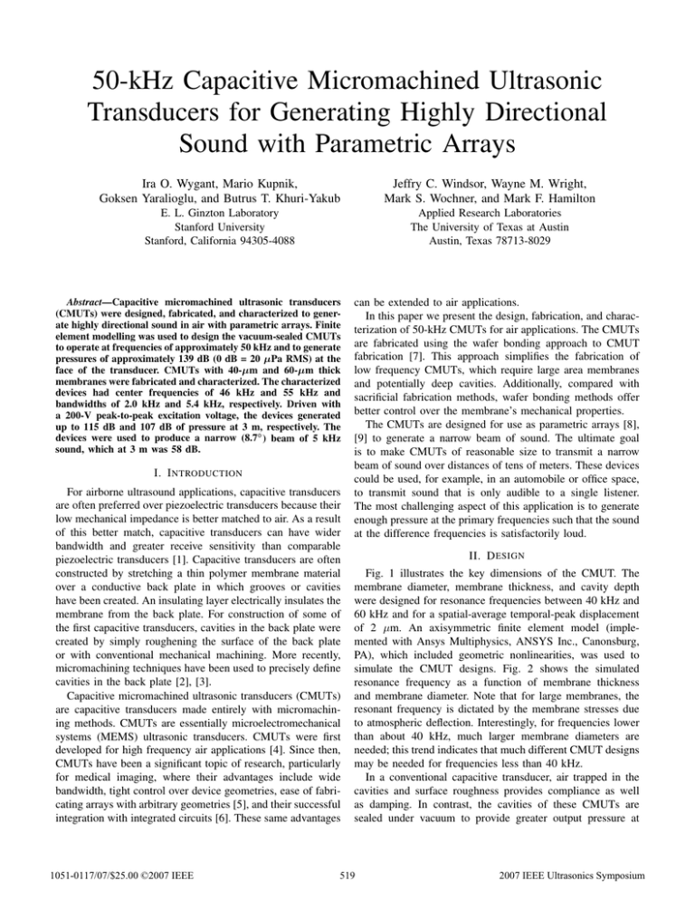
50-kHz Capacitive Micromachined Ultrasonic Transducers for Generating Highly Directional Sound with Parametric Arrays Ira O. Wygant, Mario Kupnik, Goksen Yaralioglu, and Butrus T. Khuri-Yakub Jeffry C. Windsor, Wayne M. Wright, Mark S. Wochner, and Mark F. Hamilton E. L. Ginzton Laboratory Stanford University Stanford, California 94305-4088 Applied Research Laboratories The University of Texas at Austin Austin, Texas 78713-8029 Abstract—Capacitive micromachined ultrasonic transducers (CMUTs) were designed, fabricated, and characterized to generate highly directional sound in air with parametric arrays. Finite element modelling was used to design the vacuum-sealed CMUTs to operate at frequencies of approximately 50 kHz and to generate pressures of approximately 139 dB (0 dB = 20 µPa RMS) at the face of the transducer. CMUTs with 40-µm and 60-µm thick membranes were fabricated and characterized. The characterized devices had center frequencies of 46 kHz and 55 kHz and bandwidths of 2.0 kHz and 5.4 kHz, respectively. Driven with a 200-V peak-to-peak excitation voltage, the devices generated up to 115 dB and 107 dB of pressure at 3 m, respectively. The devices were used to produce a narrow (8.7◦ ) beam of 5 kHz sound, which at 3 m was 58 dB. I. I NTRODUCTION For airborne ultrasound applications, capacitive transducers are often preferred over piezoelectric transducers because their low mechanical impedance is better matched to air. As a result of this better match, capacitive transducers can have wider bandwidth and greater receive sensitivity than comparable piezoelectric transducers [1]. Capacitive transducers are often constructed by stretching a thin polymer membrane material over a conductive back plate in which grooves or cavities have been created. An insulating layer electrically insulates the membrane from the back plate. For construction of some of the first capacitive transducers, cavities in the back plate were created by simply roughening the surface of the back plate or with conventional mechanical machining. More recently, micromachining techniques have been used to precisely define cavities in the back plate [2], [3]. Capacitive micromachined ultrasonic transducers (CMUTs) are capacitive transducers made entirely with micromachining methods. CMUTs are essentially microelectromechanical systems (MEMS) ultrasonic transducers. CMUTs were first developed for high frequency air applications [4]. Since then, CMUTs have been a significant topic of research, particularly for medical imaging, where their advantages include wide bandwidth, tight control over device geometries, ease of fabricating arrays with arbitrary geometries [5], and their successful integration with integrated circuits [6]. These same advantages 1051-0117/07/$25.00 ©2007 IEEE can be extended to air applications. In this paper we present the design, fabrication, and characterization of 50-kHz CMUTs for air applications. The CMUTs are fabricated using the wafer bonding approach to CMUT fabrication [7]. This approach simplifies the fabrication of low frequency CMUTs, which require large area membranes and potentially deep cavities. Additionally, compared with sacrificial fabrication methods, wafer bonding methods offer better control over the membrane’s mechanical properties. The CMUTs are designed for use as parametric arrays [8], [9] to generate a narrow beam of sound. The ultimate goal is to make CMUTs of reasonable size to transmit a narrow beam of sound over distances of tens of meters. These devices could be used, for example, in an automobile or office space, to transmit sound that is only audible to a single listener. The most challenging aspect of this application is to generate enough pressure at the primary frequencies such that the sound at the difference frequencies is satisfactorily loud. II. D ESIGN Fig. 1 illustrates the key dimensions of the CMUT. The membrane diameter, membrane thickness, and cavity depth were designed for resonance frequencies between 40 kHz and 60 kHz and for a spatial-average temporal-peak displacement of 2 µm. An axisymmetric finite element model (implemented with Ansys Multiphysics, ANSYS Inc., Canonsburg, PA), which included geometric nonlinearities, was used to simulate the CMUT designs. Fig. 2 shows the simulated resonance frequency as a function of membrane thickness and membrane diameter. Note that for large membranes, the resonant frequency is dictated by the membrane stresses due to atmospheric deflection. Interestingly, for frequencies lower than about 40 kHz, much larger membrane diameters are needed; this trend indicates that much different CMUT designs may be needed for frequencies less than 40 kHz. In a conventional capacitive transducer, air trapped in the cavities and surface roughness provides compliance as well as damping. In contrast, the cavities of these CMUTs are sealed under vacuum to provide greater output pressure at 519 2007 IEEE Ultrasonics Symposium Membrane Diameter Oxide Thickness TABLE I D ESIGN PARAMETERS Membrane Thickness Design Membrane diameter (mm) Membrane thickness (µm) Cavity depth (µm) Oxide thickness (µm) Cavity Depth Fig. 1. The key dimensions for the design of the CMUT are the membrane diameter, membrane thickness, and cavity depth. Highly-Doped Silicon A 4 40 36 3.3 B 4 60 16 3.3 Aluminum SiO2 Low Resistivity Silicon Wafer (a) Etched Cavity (15–30 m Deep) (b) Handle Layer (Approx. 400 m Thick) Fig. 2. A finite element model of the CMUT was used to predict resonance frequency as a function of membrane thickness and membrane diameter. Device Layer (Low Resistivity, 40-60 m Thick) the expense of bandwidth. Because the cavity is sealed under vacuum, the membranes are deflected by atmospheric pressure. The amount of this deflection is considered when choosing the cavity depth. The cavity depth must be deep enough to accommodate this deflection and the desired displacement with enough extra room to prevent pull-in at large displacements. We targeted a peak displacement of about 2-µm averaged over the membrane’s total area. Designs with 40-µm and 60-µm thick membranes were fabricated (Table I). (c) Aluminum Electrical Contact Membrane / Top Electrode (40-60 m Thick) Cavity (15-30 m Thick) Bottom Electrode III. FABRICATION (d) Membrane Center Deflection (µm) The CMUTs are fabricated using a process based on wafer bonding (Fig. 4). The fabrication process starts with a low resistivity silicon wafer. The resistivity should be low enough 50 Fig. 4. The CMUTs were fabricated using a process based on wafer bonding. (a) The process starts with a low resistivity silicon wafer. (b) The cavities are etched and oxidized. (c) The wafer with the cavities is bonded to a siliconon-insulator (SOI) wafer. (d) The handle and buried oxide layers of the SOI wafer are removed and aluminum electrodes are deposited. 40 µ m 40 Designs which were fabricated. 30 50 µ m 60 µ m 20 70 µ m 80 µ m 90 µ m 100 µ m 10 0 1000 SOI Wafer Buried Oxide Layer 1500 2000 Membrane Radius 2500 Fig. 3. Because the CMUT’s cavities are sealed under vacuum, the membrane is deflected by atmospheric pressure. The amount of this deflection is considered when choosing the cavity depth. A finite element model was used to predict the amount of deflection at the center of the membrane. such that the entire wafer can be considered electrically connected. Cavities are etched (Multiplex Pro ASE HRM Deep Reactive Ion Etcher, Surface Technology Systems, Newport, United Kingdom) in the wafer using deep reactive ion etching (DRIE). DRIE is used because it is a simple way to create deep cavities. The drawback is that the cavity depth depends on the position of the cavity relative to the wafer edge and the amount of surrounding silicon being etched. Excluding those cavities at the very edge of the wafer, the cavity depths are within 6% of the mean cavity depth. The cavities at the edge are about 10% to 12% deeper than the mean depth. Next, an insulating layer of oxide is grown. In our experience, oxide grown in our facilities has a breakdown voltage 520 2007 IEEE Ultrasonics Symposium 100 mm Membrane Bottom Electrode Fig. 5. A photo of a completed device. 15 m of approximately 400 V/µm. For these devices, we use a 3.3µm-thick layer of oxide to accommodate large DC bias and AC excitation voltages. The oxidized wafer is then wafer bonded to an SOI wafer. The bonding is done using specialized wafer bonding equipment (model SB6 wafer bonder, Karl Suss, Garching, Germany) at a temperature of 50◦ C, with a force of 600 N, and at a pressure of less than 10−5 mbar. The bonded wafers are then annealed at 1050◦ C in a dry oxidation furnace. The handle and buried oxide layers of the SOI wafer are then removed. Wafer grinding is used to remove all but 150 µm of the handle layer. The remaining handle layer is removed with tetramethylammonium hydroxide (TMAH). The buried oxide layer is then removed in a plasma etcher (AMT 8100, Applied Materials Inc., Santa Clara, Ca). Finally, aluminum is evaporated and patterned on both sides of the device to make electrodes. Because the membrane silicon and back plate silicon are low resistivity, electrical contact to the device can be made with just a few spots of aluminum. Fig. 5 is a picture of the finished device. While the fabrication process is relatively simple, it was challenging to make defect-free devices. Particles or spots of photoresist that remained in the cavity region prior to the cavity etching resulted in pillars of unetched silicon (Fig. 6). The first fabricated devices had about 30 of these pillars per wafer. These pillars disrupt membrane deflection and if not covered with thick oxide, as was the case in the devices initially fabricated, can short the bottom and top electrodes of the CMUT. Most of the pillars were a result of unexposed photoresist. We were able to eliminate most of unexposed photoresist using two exposures for the lithography step. Between the two exposures, the mask was cleaned and rotated. Rotating the mask, which was symmetric, ensures that any defects on the mask will not transfer to the wafer. The second step taken to prevent the pillars was to use isotropic DRIE to create the cavities. The isotropic etch undercuts small defects in the cavity areas. Most wafers processed using two exposures and with isotropic cavity etching had no observable pillars. IV. C HARACTERIZATION Devices fabricated according to the parameters given in Table I were characterized. Fig. 7 shows their input impedance. Silicon Pillars 7 m Fig. 6. Particles or unexposed photoresist in the cavity region prior to the cavity etch shield the etching and result in pillars of unetched silicon. These pillars disrupt the membrane’s deflection and can short the device if not covered with thick oxide. To prevent the pillars, the cavity photolithography and etch steps were modified. Fig. 7. The input impedances of devices with parameters given in Table I were measured. There are strong resonances at 45 kHz and 53 kHz for designs A and B, respectively. There also appear to be other smaller resonances, which could be a result of the cavities being deeper at the wafer’s edge than at the center. For a given bias voltage, a membrane with a deeper cavity experiences less spring softening and thus resonates at a higher frequency. A laser interferometer (model OFV-2700 controller with OVD05 decoder, Polytec, Waldbronn, Germany) measurement of the membrane deflection at difference locations on the wafer confirms that membranes at the edge resonate at a higher frequency. The devices were mounted on a rotation stage and their output was measured with a calibrated microphone (1/4” Free Field Microphone Type 40 BF, G.R.A.S. Sound and Vibration, Vedbaek, Denmark). The devices were driven with a 200V peak-to-peak AC excitation signal, which was the largest voltage that could be produced with our voltage source. The frequency responses of the devices were determined by mea- 521 2007 IEEE Ultrasonics Symposium -15° 0 0° 30° Normalized Pressure (dB) -30° Fig. 8. To measure the CMUTs’ frequency response, the on-axis pressure was measured for different excitation frequencies at a distance of 3 m. TABLE II S UMMARY OF M EASURED R ESULTS Design AC excitation (V peak-to-peak) DC bias (V) Center frequency (kHz) Bandwidth (kHz) Pressure at 3 m (dB, 0 dB = 20 µPa RMS) Pressure normalized to 0 m (dB) A 200 380 46 2.0 115 136 B 200 350 55 5.4 107 128 15° -10 -20 5-kHz Difference Frequency 50-kHz Primaries Diffraction at 5-kHz -30 -40 Fig. 9. A CMUT was used to generate a parametric array by driving it with the sum of 52 kHz and 57 kHz signals. Because of the parametric array effect, the 5-kHz difference frequency beam pattern is much narrower than the beam pattern expected for sound directly transmitted at 5 kHz. suring their output at 3 m for different excitation frequencies. The on-axis pressure was measured at a distance of 3 m. The effective source level on the face of the transducer is determined by projecting the pressure measured at 3 m back to the transducer by assuming small-signal radiation by a circular source with uniform amplitude. The results of the frequency response and output pressure measurements are given in Table II. A Design B (Table I) device was used to generate a parametric array by driving it with the sum of 52 kHz and 57 kHz 100-V peak-to-peak signals. The beam widths of the primary frequencies and the 5-kHz difference frequency were measured. The primary beam patterns are consistent with the 8-cm source size. The difference frequency beam width is 8.7◦ , which, because of the parametric array effect, is substantially narrower than the expected beam width for transmission directly at 5 kHz. For effective source pressures at the primary frequencies of 100 dB (0 dB = 20 µPa RMS) and 110 dB, the sound level of the 5 kHz difference frequency was 58 dB at 3 m, which was clearly audible. V. C ONCLUSION We fabricated large area, low frequency CMUTs for airborne applications. The fabricated devices were used to create parametric arrays to generate narrow beams of sound at 5 kHz. Ideally the CMUTs would be used to transmit speech over distances of tens of meters. Transmitting speech is particularly challenging at the lower frequencies because the primary pressures needed to achieve a certain pressure at the difference frequency is inversely proportional to the difference frequency. To generate higher pressures at distance, several devices could be combined to create a source with a larger area. A straightforward way of increasing the source pressure would be to increase the cavity depths of the device so that they could be operated with larger AC and DC voltages. Ongoing work includes designing devices that can be tiled together and that can generate larger pressures. ACKNOWLEDGMENT This work was supported by SPAWAR Grant N66001-061-2032. Work was performed in part at the Stanford Nanofabrication Facility (a member of the National Nanotechnology Infrastructure Network) which is supported by the National Science Foundation under Grant ECS-9731293, its lab members, and the industrial members of the Stanford Center for Integrated Systems. R EFERENCES [1] A. Gachagan, G. Hayward, S. Kelly, and W. Galbraith, “Characterization of air-coupled transducers,” Ultrasonics, Ferroelectrics and Frequency Control, IEEE Transactions on, vol. 43, no. 4, pp. 678–689, 1996. [2] K. Suzuki, K. Higuchi, and H. Tanigawa, “A silicon electrostatic ultrasonic transducer,” Ultrasonics, Ferroelectrics and Frequency Control, IEEE Transactions on, vol. 36, no. 6, pp. 620–627, 1989. [3] D. Schindel, D. Hutchins, L. Zou, and M. Sayer, “The design and characterization of micromachined air-coupled capacitance transducers,” Ultrasonics, Ferroelectrics and Frequency Control, IEEE Transactions on, vol. 42, no. 1, pp. 42–50, 1995. [4] M. Haller and B. Khuri-Yakub, “A surface micromachined electrostatic ultrasonic air transducer,” Ultrasonics, Ferroelectrics and Frequency Control, IEEE Transactions on, vol. 43, no. 1, pp. 1–6, 1996. [5] D. Yeh, O. Oralkan, I. Wygant, M. O’Donnell, and B. Khuri-Yakub, “3-d ultrasound imaging using a forward-looking cmut ring array for intravascular/intracardiac applications,” Ultrasonics, Ferroelectrics and Frequency Control, IEEE Transactions on, vol. 53, no. 6, pp. 1202–1211, 2006. [6] I. Wygant, et al., “Integration of 2D cmut arrays with front-end electronics for volumetric ultrasound imaging.” Accepted for publication IEEE Transactions on Ultrasonics, Ferroelectrics, and Frequency Control, 2007. [7] A. Ergun, Y. Huang, X. Zhuang, O. Oralkan, G. Yaralioglu, and B. KhuriYakub, “Capacitive micromachined ultrasonic transducers: fabrication technology,” Ultrasonics, Ferroelectrics and Frequency Control, IEEE Transactions on, vol. 52, no. 12, pp. 2242–2258, 2005. [8] P. J. Westervelt, “Parametric acoustic array,” Journal of the Acoustical Society of America, vol. 35, no. 4, pp. 535–537, 1963. [9] M. F. Hamilton and D. T. Blackstock, Nonlinear Acoustics. New York: Academic Press, 1998. 522 2007 IEEE Ultrasonics Symposium


