DATA SHEET:
CKRF7514MM34
12GHz Low Noise FET in Dual mold Plastic PKG
Features:
Description:
Low noise figure and high associated gain
Low Noise and High Gain
Original Dual mold Plastic package
NF=0.42dB TYP., Ga=12.2dB TYP.
@VDS=2V, ID=10mA, f=12GHz
Low Gain version of CKRF7513MM34
Applications:
DBS LNB gain-stage, Mix-stage
Low noise amplifier for microwave
communication system
Package:
Flat-lead 4-pin thin-type super minimold
package
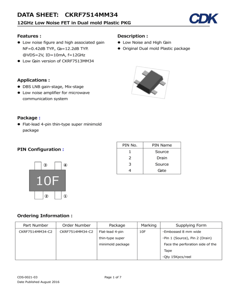
PIN Configuration:
PIN No.
PIN Name
1
Source
2
Drain
3
Source
4
Gate
10F
Ordering Information:
Part Number
Order Number
CKRF7514MM34-C2
CKRF7514MM34-C2
Package
Flat-lead 4-pin
thin-type super
minimold package
Marking
10F
Supplying Form
・Embossed 8 mm wide
・Pin 1 (Source), Pin 2 (Drain)
Face the perforation side of the
Tape
・Qty 15Kpcs/reel
CDS-0021-03
Date Published August 2016
Page 1 of 7
DATA SHEET:
CKRF7514MM34
12GHz Low Noise FET in Dual mold Plastic PKG
Absolute Maximum Ratings:
(TA=+25℃, unless otherwise specified)
Parameter
Symbol
Rating
Unit
Drain to Source Voltage
VDS
4.0
V
Gate to Source Voltage
VGS
-3.0
V
Drain Current
ID
IDSS
mA
Gate Current
IG
80
μA
Total Power Dissipation
Ptot
125
mW
Channel Temperature
Tch
+150
℃
Storage Temperature
Tstg
-55 to +125
℃
Operation temperature
Top
-55 to +125
*1
℃
*1 : Relationship of Ambient Temperature and Total Power Dissipation, please refer to the Page 3
Recommended Operating Range:
(TA=+25℃, unless otherwise specified)
Parameter
Symbol
MIN.
TYP.
MAX.
Unit
Drain to Source Voltage
VDS
+1
+2
+3
V
Drain Current
ID
5
10
15
mA
Electrical Characteristics:
(TA=+25℃, unless otherwise specified)
Parameter
Symbol
Condition
MIN.
TYP.
MAX.
Unit
Gate to Source Leak Current
IGSO
VGS=-3.0V
-
0.4
10
μA
Saturated Drain Current
IDSS
VDS=2V, VGS=0V
27
47.5
68
mA
VGS(off)
VDS=2V, ID=120μA
Transconductance
Gm
VDS=2V, ID=10mA
54
69
-
mS
Noise Figure
NF
VDS=2V, ID=10mA,
-
0.42
0.62
dB
Associated Gain
Ga
f=12GHz
10.5
12.2
-
dB
Gate to Source Cut-off Voltage
CDS-0021-03
Page 2 of 7
-1.10 -0.75 -0.39
V
DATA SHEET:
CKRF7514MM34
12GHz Low Noise FET in Dual mold Plastic PKG
TYPICAL CHARACTERISTICS:
(TA=+25℃, unless otherwise specified)
TOTAL POWER DISSIPATION
DRAIN CURRENT vs.
vs. AMBIENT TEMPERATURE
DRAIN TO SOURCE VOLTAGE
DRAIN CURRENT vs.
MINIMUM NOISE FIGURE &
GATE TO SOURCE VOLTAGE
ASSOCIATED GAIN vs. DRAIN CURRENT
CDS-0021-03
Page 3 of 7
DATA SHEET:
CKRF7514MM34
12GHz Low Noise FET in Dual mold Plastic PKG
S-Parameters:
S-parameters/Noise parameters are provided on the CDK Web site.
[Original Products] → [Low Noise GaAsFET] → [Device Parameters]
URL http://www.en.cdk.co.jp/products/highfrequency/rf/
RF Measuring Layout Pattern:
RF Measuring Layout Patterns are provided on the CDK Web site.
[Original Products] → [Low Noise GaAsFET] → [Design Support] →
[Evaluation Board Information]
URL http://www.en.cdk.co.jp/products/highfrequency/rf/designsupport/index.html
Package Dimensions:
CDS-0021-03
Page 4 of 7
DATA SHEET:
CKRF7514MM34
12GHz Low Noise FET in Dual mold Plastic PKG
Recommended Soldering Conditions:
Recommended Soldering Conditions are provided on the CDK Web site.
[Original Products] → [Low Noise GaAsFET] → [Design Support] → [others]
URL http://www.en.cdk.co.jp/products/highfrequency/rf/designsupport/index.html
CDS-0021-03
Page 5 of 7
DATA SHEET:
CKRF7514MM34
12GHz Low Noise FET in Dual mold Plastic PKG
[CAUTION]
・ All information included in this document is current as of the date this document is issued. Such information, however,
is subject to change without any prior notice.
・
You should not alter, modify, copy, or otherwise misappropriate any CDK product, whether in whole or in part.
・
CDK does not assume any liability for infringement of patents, copyrights, or other intellectual property rights of third
parties by or arising from the use of CDK products or technical information described in this document. No license,
express, implied or otherwise, is granted hereby under any patents, copyrights or other intellectual property rights
of CDK or others.
・ Descriptions of circuits, software and other related information in this document are provided only to illustrate the
operation of semiconductor products and application examples. You are fully responsible for the incorporation of
these circuits, software, and information in the design of your equipment.
CDK assumes no responsibility for any
losses incurred by you or third parties arising from the use of these circuits, software, or information.
・ CDK has used reasonable care in preparing the information included in this document, but CDK does not warrant that
such information is error free. CDK assumes no liability whatsoever for any damages incurred by you resulting from
errors in or omissions from the information included herein.
・ Although CDK endeavors to improve the quality and reliability of its products, semiconductor products have specific
characteristics such as the occurrence of failure at a certain rate and malfunctions under certain use conditions.
Please be sure to implement safety measures to guard them against the possibility of physical injury, and injury or
damage caused by fire in the event of the failure of a CDK product, such as safety design for hardware and software
including but not limited to redundancy, fire control and malfunction prevention, appropriate treatment for aging
degradation or any other appropriate measures
Because the evaluation of microcomputer software alone is very difficult, please evaluate the safety of the final
products or system manufactured by you.
・ Please use CDK products in compliance with all applicable laws and regulations that regulate the inclusion or use of
controlled substances, including without limitation, the EU RoHS Directive.
CDK assumes no liability for damages or losses occurring as a result of your noncompliance with applicable laws and
regulations.
・ This document may not be reproduced or duplicated, in any form, in whole or in part, without prior written consent of
CDK.
・ Please contact a CDK if you have any questions regarding the information contained in this document or CDK products,
or if you have any other inquiries.
CDS-0021-03
Page 6 of 7
DATA SHEET:
CKRF7514MM34
12GHz Low Noise FET in Dual mold Plastic PKG
[Caution in the gallium arsenide (GaAs) product handling]
This product uses gallium arsenide (GaAs) of the toxic substance appointed in laws and ordinances.
GaAs vapor and powder are hazardous to human health if inhaled or ingested.
・ Do not dispose in fire or break up this product.
・ Do not chemically make gas or powder with this product.
・ When discard this product, please obey the law of your country.
・ Do not lick the product or in any way allow it to enter the mouth.
[CAUTION]
Although this device is designed to be as robust as possible, ESD (Electrostatic Discharge) can damage
this device. This device must be protected at all times from ESD. Static charges may easily produce
potentials of several kilovolts on the human body or equipment, which can discharge without
detection. Industry-standard ESD precautions should be used at all times.
CHUO DENSHI KOGYO CO., LTD
3400, Matsubase-machi Koyama, Uki-shi,
Kumamoto, 869-0512, JAPAN
Tel
: +81-964-32-2730
Fax
: +81-964-32-3549
URL
: http://www.cdk.co.jp/
Contact info for inquiries
Electronic Devices Division
Sales and Planning Department
Tel
: +81-964-32-2750
E-mail
: info@cdk.co.jp
FAX
: +81-964-32-3549
CDS-0021-03
Page 7 of 7
© 2016 CHUO DENSHI KOGYO CO., LTD. All rights reserved.
