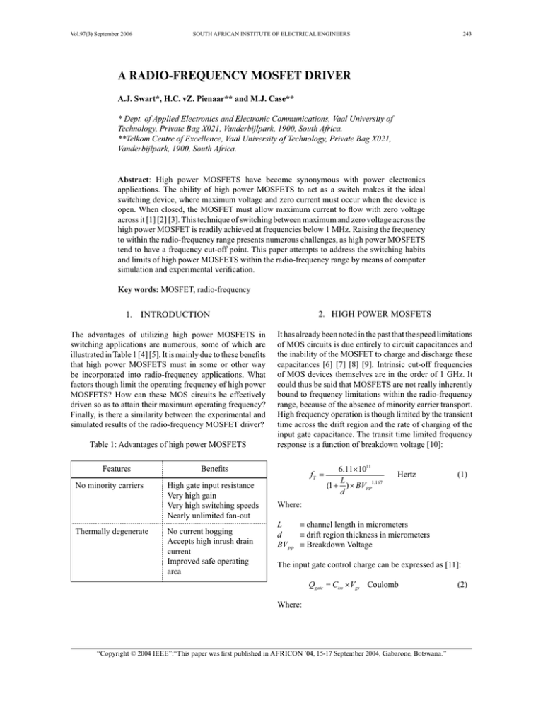
Vol.97(3) September 2006
SOUTH AFRICAN INSTITUTE OF ELECTRICAL ENGINEERS
243
A RADIO-FREQUENCY MOSFET DRIVER
A.J. Swart*, H.C. vZ. Pienaar** and M.J. Case**
* Dept. of Applied Electronics and Electronic Communications, Vaal University of
Technology, Private Bag X021, Vanderbijlpark, 1900, South Africa.
**Telkom Centre of Excellence, Vaal University of Technology, Private Bag X021,
Vanderbijlpark, 1900, South Africa.
Abstract: High power MOSFETS have become synonymous with power electronics
applications. The ability of high power MOSFETS to act as a switch makes it the ideal
switching device, where maximum voltage and zero current must occur when the device is
open. When closed, the MOSFET must allow maximum current to flow with zero voltage
across it [1] [2] [3]. This technique of switching between maximum and zero voltage across the
high power MOSFET is readily achieved at frequencies below 1 MHz. Raising the frequency
to within the radio-frequency range presents numerous challenges, as high power MOSFETS
tend to have a frequency cut-off point. This paper attempts to address the switching habits
and limits of high power MOSFETS within the radio-frequency range by means of computer
simulation and experimental verification.
Key words: MOSFET, radio-frequency
1.
2. HIGH POWER MOSFETS
INTRODUCTION
The advantages of utilizing high power MOSFETS in
switching applications are numerous, some of which are
illustrated in Table 1 [4] [5]. It is mainly due to these benefits
that high power MOSFETS must in some or other way
be incorporated into radio-frequency applications. What
factors though limit the operating frequency of high power
MOSFETS? How can these MOS circuits be effectively
driven so as to attain their maximum operating frequency?
Finally, is there a similarity between the experimental and
simulated results of the radio-frequency MOSFET driver?
Table 1: Advantages of high power MOSFETS
Features
No minority carriers
Thermally degenerate
It has already been noted in the past that the speed limitations
of MOS circuits is due entirely to circuit capacitances and
the inability of the MOSFET to charge and discharge these
capacitances [6] [7] [8] [9]. Intrinsic cut-off frequencies
of MOS devices themselves are in the order of 1 GHz. It
could thus be said that MOSFETS are not really inherently
bound to frequency limitations within the radio-frequency
range, because of the absence of minority carrier transport.
High frequency operation is though limited by the transient
time across the drift region and the rate of charging of the
input gate capacitance. The transit time limited frequency
response is a function of breakdown voltage [10]:
Benefits
High gate input resistance
Very high gain
Very high switching speeds
Nearly unlimited fan-out
No current hogging
Accepts high inrush drain
current
Improved safe operating
area
fT
6.11u 1011
L
(1 ) u BVPP1.167
d
Hertz
(1)
Where:
L
{ channel length in micrometers
d
{ drift region thickness in micrometers
BVPP { Breakdown Voltage
The input gate control charge can be expressed as [11]:
Qgate
Ciss u Vgs Coulomb
Where:
“Copyright © 2004 IEEE”:“This paper was first published in AFRICON ’04, 15-17 September 2004, Gabarone, Botswana.”
(2)
244
SOUTH AFRICAN INSTITUTE OF ELECTRICAL ENGINEERS
Ciss { the input capacitance, in pico farad, being the sum
of CGS (the gate to source capacitance) and CDG (the
drain to gate capacitance)
Vgs { gate to source voltage
The power required then to drive the gate of the MOSFET
is given by [11]:
PGate
0.5 u Ciss u Vgs 2 u f Watts
(3)
Vol.97(3) September 2006
The circuit diagram of the experimental model, shown in
Figure 2, features two separate complementary emitter
stages coupled in series, one utilizing a BC639 and BC640,
the other a TIP31C and TIP32C. The BC639 and BC640
both have an fT of 100 MHz while being able to source 1
A of current. Total power dissipation is around 800 mW
[16]. The IRF610 high power MOSFET has a Ciss of 140
pF [17]. From equation 3 then, the following gate drive
power would be required if Vgs is 12 V and the operating
frequency is set at 7 MHz:
Where:
0.5 u 140 u 109 u 122 u 7 u 106
70 mW
f { input frequency in Hertz
PGate
PGate
The high power MOSFET is in reality a bulk semiconductor,
where a gate potential controls the majority-carrier current
[4]. The fundamental issue is thus to pump charge into the
gate of the MOSFET and then to quickly withdraw it again.
This must occur at a rate of a few nanoseconds and at a gate
voltage of between 0 and 10 V, so as to enable the MOSFET
device to operate correctly within the radio-frequency range
[12]. The maximum input gate voltage must not exceed 15
V [13]. It has been documented that high power MOSFETS
can achieve switching speeds of 100 ns or less when driven
from a gate drive circuit with a low output impedance,
being able to sink and source relatively large currents [13].
The complementary emitter follower is an example of such
a gate drive circuit. More recently though, a practical gate
drive circuit was designed and built in conjunction with
a frequency synthesizer operating between 100 kHz and
8 MHz. This gate drive circuit utilized a complementary
emitter follower and proved very successful in driving the
gate of a high power MOSFET [14].
Figure 1: An example of a complementary emitter
follower
3.
COMPLEMENTARY EMITTER FOLLOWER
Operating a high power MOSFET as a switch requires a
change between the lowest and highest resistance states
of the device in the shortest possible time. Ultimately the
switching performance of the MOSFET is determined by
how quickly the voltages can be changed across the gate
input capacitances, which are the sum of the gate to source
capacitance and the drain to gate capacitance [11] [8]. It
may be shown that this can be done with a complementary
emitter follower, an example of which is sketched in Figure
1. If positively pulsed, VCC is directly coupled to the gate
via T1 with hardly any series resistance. When the pulse is
zero, T2 conducts and shorts the gate of the MOSFET to
ground with again virtually zero resistance.
Two further noteworthy properties of the complementary
emitter follower is firstly that the two base-emitter junctions
protect each other against reverse breakdown and secondly
it does not require any Schottky diode for reverse current
protection [15].
75
R1
B
Q2
BC639
V1
Output
Q4
TIP31
IRF610
A
1.5u
X
Q1
L1
Q3
BC640
V2
Q5
TIP32
1k
R2
Figure 2: The schematic diagram of the complementary
emitter follower with the high power MOSFET
Vol.97(3) September 2006
SOUTH AFRICAN INSTITUTE OF ELECTRICAL ENGINEERS
However, the required gate drive power increases to
1 W when an IRFP250 MOSFET with a Ciss of 2159 pF
is utilized in the circuit [17]. For this reason a second
complementary emitter stage was included to handle higher
amounts of power dissipation required by MOSFETS with
higher input gate capacitances. The minimum fT of both the
TIP31C and TIP32C are specified to be 3 MHz according
to their respective data sheets [16].
4.
SIMULATION MODEL
follower which is connected via the 1.5 µH coil to the gate
of the high power MOSFET. The larger amplitude signal,
B, is the output from the high power MOSFET. The time
period can be seen to be 143 ns that equates to an operating
frequency of 7 MHz. The duty cycle is found to be less
than 50%. The input signal voltage is also discernable at
11.87 V, while the output across the MOSFET swings from
0 V to 16 V, which is roughly the supply voltage.
5.2 Experimental results
The SPICE model for the IRF610 high power MOSFET
was initially incorporated into the SIMETRIX simulation
software package. Figure 2 shows the circuit layout of the
MOSFET driver compiled within the simulation package.
The output frequency spectrum of the experimental model
is illustrated in Figure 4 while Figure 5 shows the time
domain signal of the experimental model as obtained form
a TEKTRONIX digital oscilloscope.
The supply voltage was initially set to 15 V. The input signal
to the first complementary emitter stage was a 7 MHz 12 V
peak square wave. A 50 % duty cycle was utilized with the
total time period being 143 ns. R2 was included to prevent
the gate of the high power MOSFET from ever floating,
which could be detrimental to the MOSFET device if
under full load conditions. The 1.5 uH coil was included in
the experimental model as too much ringing was observed
on the digital oscilloscope display. The load resistance
was varied between 50 : and 75 :, and yet did not alter
the performance of the radio-frequency MOSFET driver.
Voltage probes were included at the output of the second
complementary emitter follower as well as across the high
power MOSFET to ground.
5.
5.1
o=7045kHz, A=15.16dB x=14.09MHz, A=10.46dB
20
10
0
-10
-20
-30
-40
0
5
10
15
20
25
30
35
40
45
MHz
50
143.8225n
Closer examination of Figure 4 reveals that the second
and third harmonics are very prominent, indicating the
presence of a square wave input frequency signal. The
fourth harmonic, at 28 MHz, is significantly smaller than
the second and third with the fifth and sixth harmonic being
similar in amplitude.
B
16
14
CH2
A
10
8
11.878704V
6
Voltage 5V/div
11.898623
12
Voltage / V
o
Figure 4: The output frequency spectrum of the experimental
model
Figure 3 shows the time domain signal as obtained from
the simulated model. The smaller amplitude signal,
A, represents the output of the complementary emitter
143.8186ns
dB
RESULTS
Simulated results
3.915605p
245
4
2
0
Time/nSecs
50
100
150
200
19.91880m
250
CH1
Time 25 ns / div
50nSecs/div
Figure 3: The input and output of the high power MOSFET
as obtained from the simulation model
Figure 5: The input and output signal of the high power
MOSFET as obtained from the experimental model
246
SOUTH AFRICAN INSTITUTE OF ELECTRICAL ENGINEERS
CH1, in Figure 5, represents the output signal from the
complementary emitter follower, which is connected to
the gate of the high power MOSFET. CH2 illustrates the
output taken from across the MOSFET to ground. Note the
time period for the output signal, CH2, as being 143 ns
while its voltage is set at just less than 20 V. The input
signals voltage, CH1, is less than 15 V.
Figure 6 illustrates a significant similarity between two
output signals of the complementary emitter follower
when under load and when isolated from the load. A
comparison was also made between the output waveforms
of the simulation model and the experimental model which
is illustrated in Figure 7.
gate of the high power MOSFET, while the Y signal is
the output of the complementary emitter follower when
connected to the MOSFETS gate. Two notable differences
are discernable upon closer examination. The Y signal has
a wider falling trail and a somewhat more curved ground
voltage than the X signal has.
A comparison between the outputs of the two models,
as shown in Figure 7, also reveals some significant
differences. The experimental model shows a rise time of
around 25 ns compared to the 20 ns of the simulated model.
Similarly, fall times for the experimental model are found
to be 25 ns while the simulated model is around 15 ns. The
experimental model has a flatter supply voltage response
than that of the simulated model. On the other hand, the
simulated model’s ground response is better than that of
the experimental model.
Voltage 5 V / div
6.
X
Y
Figure 6: The output signal from the complementary emitter
follower for the following two conditions; X - isolated from
the gate of the high power MOSFET and; Y - connected to
the gate of the high power MOSFET
Voltage 5 V / div
Experimental Model
Time 25 ns / div
Time 25 ns / div
Figure 7: A comparison between the simulated and
experimental result of the output frequency signal of the
high power MOSFET
The X signal in Figure 6 represents the output of the
complementary emitter follower when isolated from the
FUTURE WORK
Experimental tests must still be carried out on the
usefulness of the IRF530 in the radio-frequency range. It
has the ability to source a larger amount of current and
dissipate more power than the IRF610 does. It does though
have a larger input gate capacitance than the IRF610 and
this could cause significant changes in the performance of
the high power MOSFET driver.
Another line of thought in driving high power MOSFETS
encompasses the idea of using a negative and positive gate
bias voltage. Pumping charge into and out of the gate of
high power MOSFETS could thus result in faster switching
times.
High speed MOSFET driver IC’s, such as the DEIC420,
are also commercially available that enable the switching
of high power MOSFETS up to around 45 MHz [18].
These packages have the disadvantage of not being as
cost-effective as the two stage complementary emitter
follower presented here. However, a correlation between
the complementary emitter follower and MOSFET driver
IC may reveal certain similarities or differences.
7.
Simulation Model
Vol.97(3) September 2006
CONCLUSION
From the above results, and in particular Figure 7, it is clear
that the experimental model and the simulated model’s
results agree significantly. Furthermore, the ability of
the high power MOSFET to operate at a radio-frequency
of 7 MHz has been shown. Although the output from the
MOSFET does not exactly resemble the input square
waveform, it does exhibit the quality of being able to switch
rapidly between ground and VCC voltage levels. Figure 6
furthermore confirms that the high power MOSFET gate
does not significantly alter the output waveform of the
complementary emitter follower.
The gate power required to switch high power MOSFETS
Vol.97(3) September 2006
SOUTH AFRICAN INSTITUTE OF ELECTRICAL ENGINEERS
on and off is primarily influenced by the frequency of
operation, gate voltage and input gate capacitance. The
complementary emitter follower is capable of operating
within the radio-frequency range of 7 MHz and of supplying
the necessary gate voltage of between 10 and 15 V. It also
has the ability to source and sink large currents required to
rapidly charge and discharge the input gate capacitances.
Both the experimental and simulated results thus confirm
that the complementary emitter follower is indeed a worthy
radio-frequency MOSFET driver.
8.
REFERENCES
[1] J.M. Doyle: Digital, Switching, and Timing Circuits,
Duxbury Press, North Scituate, Massachusetts, pp 34, 1976.
[2] B. Maurice and L. Wuidart: Drive circuits for power
MOSFETS and IGBTs, 1994, [Online], available at:
http://www.st.com/stonline/books/ascii/docs/3703.
htm, accessed 12 May 2004.
[3] A. Agarwal and J.H. Lang: Foundations of Analog
and Digital Electronic Circuits, Morgan Kaufmann
Publishers, San Francisco, pp 285-291, 2005.
[4] E. S. Oxner: Power FETS and their applications,
Prentice-Hall Inc., New Jersey, pp 5-13, 1982.
[5] T.F. Bogart, J.S. Beasley and G. Rico: Electronic
Devices and Circuits, Pearson Prentice Hall, New
Jersey, sixth edition, p 682, 2004.
[6] R.H. Crawford: MOSFET in Circuit Design, Texas
Instruments Electronics Series, McGraw-Hill, New
York, pp 3-10, 1967.
[7] M. Golio: RF and Microwave Semiconductor Device
Handbook, CRC Press, Boca Raton, pp 6.10-6.16,
2003.
247
[8] R.S. Muller, T.I. Kamins and M. Chan: Device
Electronics for Integrated Circuits, John Wiley &
Sons, New York, third edition, pp 446-461, 2003.
[9] T.H. Lee: The design of CMOS radio-frequency
integrated circuits, Cambridge University Press,
Cambridge, second edition, pp 173-176, 2004.
[10] B.J. Baliga: Modern Power Devices, John Wiley &
Sons, New York, pp 300-314, 1987.
[11] B.E. Taylor: Power MOSFET Design, Wiley,
Chichester, pp 3-4, 1993.
[12] M. Brown: Practical power supply design, Academic
Press, San Diego, p 51, 1990.
[13] A.D. Grant and J. Gower: Power MOSFETS Theory
and Applications, John Wiley & Sons, New York, pp
194-197, 1989.
[14] A.J. Swart and H.C. vZ. Pienaar: “A high frequency
MOSFET driver” presented at the SAUPEC 2004
conference, University of Stellenbosch, Stellenbosch,
January 2004.
[15] L. Balogh: Design and application guide for high
speed MOSFET gate drive circuits, Texas Instruments
Homepage, [Online], available at: http://www.ti.com,
accessed 12 June 2003.
[16] D.A.T.A BOOK: Electronic Information Series,
D.A.T.A, San Diego, twenty forth edition, pp 191,
220, 315 and 350, 1988.
[17] International Rectifier Homepage: [Online], available
at:
http://www.irf.com/product-info/datasheets/,
accessed 12 March 2004.
[18] IXYSRF Homepage: [Online], available at: http://
www.ixysrf.com/products/MOSFET_Driver_ICs.
html, accessed 12 June 2005.
