A Current-Mode Non-inverting CMOS Buck-Boost DC
advertisement

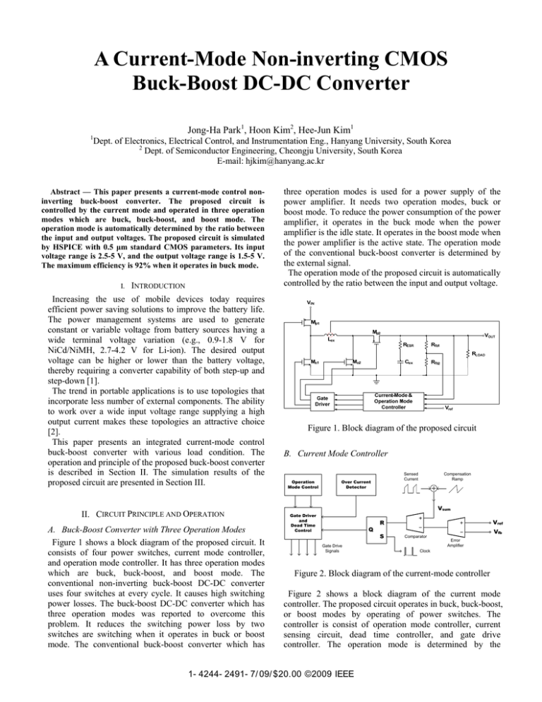
A Current-Mode Non-inverting CMOS Buck-Boost DC-DC Converter Jong-Ha Park1, Hoon Kim2, Hee-Jun Kim1 1 Dept. of Electronics, Electrical Control, and Instrumentation Eng., Hanyang University, South Korea 2 Dept. of Semiconductor Engineering, Cheongju University, South Korea E-mail: hjkim@hanyang.ac.kr Abstract — This paper presents a current-mode control noninverting buck-boost converter. The proposed circuit is controlled by the current mode and operated in three operation modes which are buck, buck-boost, and boost mode. The operation mode is automatically determined by the ratio between the input and output voltages. The proposed circuit is simulated by HSPICE with 0.5 μm standard CMOS parameters. Its input voltage range is 2.5-5 V, and the output voltage range is 1.5-5 V. The maximum efficiency is 92% when it operates in buck mode. I. INTRODUCTION Increasing the use of mobile devices today requires efficient power saving solutions to improve the battery life. The power management systems are used to generate constant or variable voltage from battery sources having a wide terminal voltage variation (e.g., 0.9-1.8 V for NiCd/NiMH, 2.7-4.2 V for Li-ion). The desired output voltage can be higher or lower than the battery voltage, thereby requiring a converter capability of both step-up and step-down [1]. The trend in portable applications is to use topologies that incorporate less number of external components. The ability to work over a wide input voltage range supplying a high output current makes these topologies an attractive choice [2]. This paper presents an integrated current-mode control buck-boost converter with various load condition. The operation and principle of the proposed buck-boost converter is described in Section II. The simulation results of the proposed circuit are presented in Section III. II. CIRCUIT PRINCIPLE AND OPERATION A. Buck-Boost Converter with Three Operation Modes Figure 1 shows a block diagram of the proposed circuit. It consists of four power switches, current mode controller, and operation mode controller. It has three operation modes which are buck, buck-boost, and boost mode. The conventional non-inverting buck-boost DC-DC converter uses four switches at every cycle. It causes high switching power losses. The buck-boost DC-DC converter which has three operation modes was reported to overcome this problem. It reduces the switching power loss by two switches are switching when it operates in buck or boost mode. The conventional buck-boost converter which has three operation modes is used for a power supply of the power amplifier. It needs two operation modes, buck or boost mode. To reduce the power consumption of the power amplifier, it operates in the buck mode when the power amplifier is the idle state. It operates in the boost mode when the power amplifier is the active state. The operation mode of the conventional buck-boost converter is determined by the external signal. The operation mode of the proposed circuit is automatically controlled by the ratio between the input and output voltage. Figure 1. Block diagram of the proposed circuit B. Current Mode Controller Operation Mode Control Sensed Current Over Current Detector Compensation Ramp Vsum Gate Driver and Dead Time Control Q Gate Drive Signals Vref R S Vfb Comparator Error Amplifier Clock Figure 2. Block diagram of the current-mode controller Figure 2 shows a block diagram of the current mode controller. The proposed circuit operates in buck, buck-boost, or boost modes by operating of power switches. The controller is consist of operation mode controller, current sensing circuit, dead time controller, and gate drive controller. The operation mode is determined by the 1-4244-2491-7/09/$20.00 ©2009 IEEE (a) Circuit diagram (b) Timing diagram Figure 3. Schematic of the dead-time and gate drive controller operation mode controller. When the operation mode is determined, it has to drive different pairs of power switches as an operation mode. Table 1 shows the state of power switches at each operation modes. In the table, two switches are driving by PWM signals when it operates in buck or boost operation mode. Four switches are driving by PWM signals, when it operates in the buck-boost mode. Figure 3 shows the schematic of the dead time controller and the gate drive controller. It makes four gate driving signals by using a PWM signal. consists of resistors, logic gates, and latches. The range of each operation mode is controlled by resistors. TABLE I. STATE OF SWITCHES AT EACH OPERATION MODE Mp1 Buck Buck-Boost Boost On On On Buck Buck-Boost Boost Off Off On Mp2 On Time On Off Off Off Time On On On Mn1 Mn2 Off Off Off Off On On On On Off Off Off Off Figure 4. Schematic of the operation mode controller Since MOSFETs are used instead of a shottkey diode, it is able to turn on p and n channel MOSFET at the same time. It causes lots of power dissipation and unstable operation of all circuitry blocks. To avoid this, the switches have to be controlled by non-overlapping signals. Figure 3 (b) shows timing diagram of the deadtime controller in the continuous current mode (CCM) and the discontinuous current mode (DCM). In the figure, Vs means the reverse current detecting signal. The deadtime controller is shown by the dashed box in the figure 3(a). C. Operation-Mode Controller Figure 4 shows a block diagram of the operation-mode controller. This circuit determines the operation mode by the ratio between the input voltage and the output voltage. It has a hysteresis to prevent the oscillation of the operation mode. If the operation mode is controlled without the hysteresis, the operation mode can oscillate at the edge of each mode. It makes that the output voltage is unstable. Figure 5 shows the transfer characteristic of the operation-mode controller. It Figure 5. Transfer characteristic of the operation mode controller. D. Current Sensing Circuit The current sensing circuit is one of the most important building blocks in current mode control. The SenseFET current sensing circuit is adapted. Figure 6 shows a schematic of the current sensing circuit. It has a high accuracy and noise performance. It can operate in low power supply voltage. And it can be easily compensated and has high speed response. In the figure 7, the current sensing circuit is shown by the dashed box. The relationship of the sensed current and the inductor current can be determined by the aspect ratio of Ms and Mp1. VIN VIN VGATE Mp1 MS (b) Buck-boost mode Lex Vsense Mn1 Vbias Figure 6. Schematic of the current sensing circuit III. SIMULATION RESULTS HSPICE simulation program was used to verify operations of the proposed circuit with 0.5μm CMOS standard process parameter. The reference voltage, VREF, is 1.2V, and peak-topeak voltage of the saw-tooth wave, VM, is 2V. The value of components are selected as the external capacitor is 10μF, the external inductor is 20μH. TABLE II. SUMMARY OF SIMULATION RESULTS Parameter Min Typ Max Units Vin 2.5 5 V Vout 1.5 5 V Iout 50mA 1.5A A fs 1.2 1.3 1.47 MHz Efficiency 92 % (c) Boost mode Figure 7. Simulated waveforms Figure 7 shows various waveforms of the proposed circuit when it operates in each mode. It shows the output voltage and operation mode control signals. The maximum efficiency is measured as 92% when it operates in the buck mode. Table 2 shows the summary of simulation results. IV. CONCLUSION This paper presents a current-mode control non-inverting CMOS buck-boost DC-DC converter with three operation modes. Its operation and performance were verified by HSPICE. The simulation results show that the proposed circuit can be applied for battery operation systems have wide supply voltage ranges. REFERENCES [1] [2] [3] (a) Buck mode Biranchinath Sahu, et al., A High-Efficiency, Dual-Mode, Dynamic, Buck-Boost Power Supply IC for Portable Applications, in proc. VLSID’05, pp. 858-861, 2005. Biranchinath Sahu, et al., A Low Voltage, Dynamic, Noninverting, Synchronous Buck-Boost Converter for Portable Applications, IEEE Trans. Power Electronics, Vol. 19, No. 2, pp. 443-452, 2004. F.-F. Ma, W.-Z. Chen, and J.-C. Wu, A Monolithic Current-Mode Buck Converter With Advanced Control and Protection Circuits, IEEE Trans. Power Electronics, Vol. 22, No. 5, pp. 1836-1846, 2007.


