Modeling and Simulation of Full-bridge Series Resonant Converter
advertisement
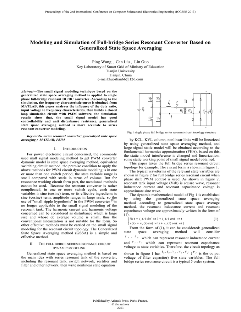
Proceedings of the 2nd International Conference on Computer Science and Electronics Engineering (ICCSEE 2013) Modeling and Simulation of Full-bridge Series Resonant Converter Based on Generalized State Space Averaging Ping Wang , Can Liu , Lin Guo Key Laboratory of Smart Grid of Ministry of Education Tianjin University Tianjin, China e-mail:huoshan66@126.com Abstract—The small signal modeling technique based on the generalized state space averaging method is applied to single phase full-bridge resonant DC/DC converter .According to the simulation, the frequency characteristic curve is obtained from MATLAB, this paper analyzes the influence of the duty ratio, input voltage to frequency characteristics, then builds a closed loop simulation circuit with PSIM software, the simulation results show that, the small signal model has good controllability and anti disturbance resistance, generalized state space averaging method is more accurate to series resonant converter modeling. Fig 1 single phase full bridge series resonant circuit topology structure Keywords- series resonant converter; generalized state space averaging ; MATLAB; PSIM I. INTRODUCTION For power electronic circuit concerned, the commonly used mall signal modeling method to get PWM converter dynamic model is state space averaging method, equivalent switching circuit method, the premise condition to apply the above methods for PWM circuit dynamic modeling is in one or more than one switch period, the state variable range is small compared with static in terms of volume. But for resonance working circuit form part, the mentioned methods cannot be used. Because the resonant converter is rather complicated, in one or more switch cycle, each state variables is sine (cosine) term, or its effective ingredients is sine (cosine) term, amplitude ranges in large scale, so the use of "small ripple hypothesis" in the PWM converter [1]is no longer applicable to the small signal modeling of the resonant tank. The harmonic current and harmonic voltage concerned can be considered as disturbance which is large size and whose dc average volume is small, thus the conventional linearization is not suitable for the form. So other effective methods must be carried on the small signal modeling for the resonant circuit topology. The Generalized State Space Averaging method (GSSA) is a simple and effective method. II. THE FULL BRIDGE SERIES RESONANCE CIRCUIT DYNAMIC MODELING Generalized state space averaging method is based on the main idea with series resonant tank of the converter, including the resonant tank, switch network, rectifier and filter and other network, then write nonlinear state equation by KCL, KVL column, nonlinear links will be linearized by using generalized state space averaging method, and large signal static model will be obtained according to the fundamental harmonics approximation (FHA), based on this, the static model interference is changed and linearization, some static working point of small signal model obtained. This paper takes the full bridge series resonant circuit topology for example. The circuit form is shown in figure 1. The typical waveforms of the relevant state variables are shown in figure 2 for full bridge series resonant circuit when phase shift PWM control is used. As shown in figure 2, resonant tank input voltage (Vab) is square wave, resonant inductance current and resonant capacitance voltage is approximate sine wave. The dynamic mathematical model of Fig 1 is established by using the generalized state space averaging method .according to generalized state space average method, the resonant inductance current and resonant capacitance voltage are approximately written in the form of (1) . i ( t ) = i s ( t ) sin( wt ) + i c ( t ) cos( wt ) (1) v ( t ) = v s ( t ) sin( wt ) + v c ( t ) cos( wt ) From the form of (1), it can be considered: generalized state space averaging method will consider is , ic which can represent resonant inductance current and v s , v c which can represent resonant capacitance voltage as state variables. Therefore, the circuit topology as i ,i ,v ,v ,v v shown in figure 1 has s c s c f ( f is the output voltage of filter capacitor) five state variables. The full bridge series resonance circuit is a typical 5 order system. Published by Atlantis Press, Paris, France. © the authors 2263 Proceedings of the 2nd International Conference on Computer Science and Electronics Engineering (ICCSEE 2013) Through processing the (5), then we can get related amount of static results. The method is: make (5) on the left side of the differential item is equal to zero. And then solving system of equations, and ultimately the static results. Linearized and interferenced to (5), then we can get small signal model. Fig 2 Typical waveforms of the state variables of an SRC Notice that the envelop terms i s , i c , v s , v c are slowly time varying, they are varying slower than the switching frequency, so the dynamic behavior of these terms can be investigated.[2][3] For (1) use differential on both sides of the equation, can easily obtain (2). di di di = ( s − wi c ) sin( wt ) + ( c + wi s ) cos( wt ) dt dt dt dv dv s dv = ( − wv c ) sin( wt ) + ( c + wv s ) cos( wt ) dt dt dt (2) In figure 1 circuit, for simplicity, make its transformer turns ratio is n = 1 : 1 , therefore, under continuous tank current mode, we can make a list of the equation of state variables, such as (3) shows. L C C r r f di + v + sgn( i)v dt dv = i dt dv f Vf + = | i | dt R L f = v ab (3) Where sgn( x ) is symbol function, that is: 1, x > 0 sgn ( x ) = 0, x = 0 − 1, x < 0 Exerting Fourier decomposition expansion and reasonable base wave approximation for the various relevant amount[4], we may safely draw the (4) approximation results. π 4 vab (t ) = π sin( 2 d )vg sin(wt ) sgn(i )v = 4 is v sin(wt ) + 4 ic v cos(wt ) (4) f f f π ip π ip 2 | i |≈ i p π i = i 2 + i 2 s c p By substituting (2) (4) into (3), and by equating the coefficients of dc. sine and cosine terms respectively, we get a 5 order state equation. Lr Lr C r C r C f di s 4 is 4 π = L r wi c − v s − v f + sin( d ) v g dt 2 π ip π di c 4 ic = − L r wi s − v c − vf dt π ip (5) dv s = C r wv c + i s dt dv c = − C r wv s + i c dt dv f vf 2 = ip − dt π RL We assume that all relevant variables static stable value I s , I c ,V s ,V c ,V f , D ,V g ,W is: . The D is static duty ratio, W is static switch frequency (angular frequency). Linearized and interferenced to (5). As it is common to control the system with fixed frequency and variable duty ratio (phase-shifting Angle), so here only duty ratio is linearized and interferenced, and filter capacitor voltage is taken as output. In the process of the linearization and interference, to contain state variables of the nonlinear part multiplied by reasonable Taylor series expansion and partial differential approximate,[5] finally can get small signal equation of state matrix and output matrix (6). − 4 I c2V f 3 π Lr I p 4 I s I cV f −W 3 π Lr I p 1 A= Cr 0 2Is πC f I p W + 4 I s I cV f πLr I 3p − 4 I s2V f − 1 Lr − 0 − 1 Lr − πLr I 3p 0 0 0 w 1 Cr 2Ic πC f I p −w 0 0 0 π 2V g cos( 2 D ) Lr 0 B = 0 0 0 4Is πLr I p 4Ic (6a) πLr I p 0 1 − R L C f 0 (6b) (6c) C = [0 0 0 0 1] According to the relationship between (6) to transfer function of small signal model, the transfer function (7) of v the output C to the control variable duty ratio d can be easily obtained . (7) G d ( s ) = C ( sI − A ) − 1 B f Published by Atlantis Press, Paris, France. © the authors 2264 Proceedings of the 2nd International Conference on Computer Science and Electronics Engineering (ICCSEE 2013) III. SIMULATION RESULTS In figure 1 circuit, the correctness of the theoretical analysis will be proved after the simulation test. the simulation parameters are: V g = 100 V , L r = 197 μ H , C r = 50 nF , D = 0 .8 R L = 10 Ω V f = 100 uF a) D=0.2 Transformer turn ratio is: N 1 : N 2 = 1 : 1 Resonance frequency is: 1 fr = 2π LrC r = 50 . 6 kHz For the given simulation parameters concerned, open loop system BODE corresponding curve can be easily drawn by using mathematical analysis software MATHCAD and MATLAB, as shown in figure 3.1. A. Simulation of open-loop system In order to achieve the effect of ZVS soft switch,[6] the switch frequency f s is slightly greater than the resonance frequency f r , here take f s = 55 kHz From the second part of the theoretical deducing process, it can be concluded that D = 0.8, output voltage Vf approximation is 58v. After the analysis and simulation of the frequency characteristic curve, it is not difficult to discover that, the duty ratio - the output frequency characteristic of series resonant converter ,in low frequency band the curve is a horizontal line, in the mid frequency band the curve crosses 0 dB place by the slope of − 20 dB / dec , in high frequency band by slope − 40 dB / dec attenuation, so it can be equivalent to a system which consists of a proportional link, a first-order inertia link and a secondorder oscillation link. From (6) and (7), the conclusion can be obtained that when the hard-ware and switching frequency of the system is confirmed, the parameters which can have effects on the system are only duty-cycle D and the input voltage Vg. So, the change of the system performance is analyzed when D and Vg changes. The bode diagrams of the open-loop system are illustrated separately in Fig 3.2 as D=0.2 and D=0.5. b) D=0.5 Fig 3.2 the open-loop bode diagram as D=0.2 and D=0.5 The Fig 3.1 and Fig 3.2, indicates that the change of D can only result in the change of the gain of the open-loop system, and the phase-frequency characteristic will not change. Also, the bode diagram changes along with the change of Vg in a similar way. The following figure 3.3 shows the output voltage waveform after the simulation to the system by using PSIM simulation software. The figure 3.3shows, output voltage Vf static stability values accord with theoretical analysis and 58v results. B. Design and Simulation of close-loop system The concept of three frequency band is used here for the design of close-loop system. The three frequency band could be described as: To the close-loop system, its openloop bode diagram should be designed as follows: the gain of the low frequency should be high to reduce the steadystate error; In the mid-frequency band, the curve should cross the 0 dB by the slope of − 20 dB / dec and the width of the mid-frequency band should be long; The slope of the high-frequency band should be at least − 40 dB / dec to enhance resistance to disturbance performance. So, the PI regulator can be designed as : Figure 3.1 open loop system BODE diagram Figure 3.3 open loop system output voltage waveform Published by Atlantis Press, Paris, France. © the authors 2265 Proceedings of the 2nd International Conference on Computer Science and Electronics Engineering (ICCSEE 2013) Fig 3.4 the control block diagram of close-loop system b) the steady-state voltage ripple Fig 3.7 the voltage waveform of the close-loop system IV. Fig 3.5 the bode diagram of close-loop system 0 .7 ( s + 1000 ) s (8) Then, the control block diagram is illustrated in Figure 3.4. The MATLAB is used to get the open-loop bode diagram of the close-loop system in Figure 3.4 The PSIM is used to simulate and verify the system. The schematic of system is Fig 3.6,The output voltage Vo is in Fig 3.7, The Fig 3.7 indicates that the performance of the close-loop system has good controllability and anti disturbance resistance. CONCLUSION The small-signal modeling technique based on Generalized State Space Averaging can be applied to the Series Resonant DC/DC Converters. In this paper, the smallsignal model of an open loop single phase full bridge series resonant converter is built and the closed loop system for this open loop system is also designed by using MATHCAD and MATLAB. The open loop and closed loop systems are simulated and authentication with PSIM. According to the simulation, the steady-state output of the open loop system fits well with theoretical calculation, and the closed loop system can also meet the needs of disturbance resistance. Concluded from the Mathematical analysis and the simulation of power electronic circuits, Generalized State Space Averaging is suitable for the PWM converter with resonant circuits. ACKNOWLEDGMENT This paper is supported by the Specialized Research Fund for the Doctoral Program of Higher Education of China (2012003211070). REFERENCES Fig 3.6 the schematic of close-loop system [1] Weiping Zhang, The model and control of switch converter. Beijing: Electric Power Publishing House,2005.pp.285-300 [2] S. Sanders, J. Noworolski, X.Z. Liu, and G. Verghese, "Generalized averaging method for power conversion circuits," Power Electronics Specialists Conference, 1990. PESC '90 Record., 21st Annual IEEE ,pp.333-340, Jun 1990. [3] F. Silveira Cavalcante, and J. Kolar, “Small-Signal Model of a 5kW High-Output Voltage Capacitive-Loaded Series-Parallel Resonant DC-DC Converter,” Power Electronics Specialists Conference 2005.,pp.1271-1277, Jun 2005. [4] Divan D M, "The resonant DC link converters a new concept in static power conversion. EEE Trans Ind Applicat,1989,25(2):3 17-325 [5] Weiping Zhang, Peng Mao, and Yuanchao Liu “Small-Signal Modeling of Series Resonant Converter” PEDS 2007 [6] V. Vorperian, "Approximate Small-Signal Analysis of the Series and the Parallel Resonant Converters," IEEE Transaction on Power Electronics, Vol. 4, No. 1, pp.15-24, January 1989. [7] Seth R.Sanders, J. Mark Noworolski, Xiaojun Z.Liu, andGeorge C.Verghese "Generralized Averaging Method for Power Conversion Circuits" IEEE Transaction on Power Electronics,Vol.6,No.2,pp.251259,April 1991. a) the time response of the system Published by Atlantis Press, Paris, France. © the authors 2266
