Study of oxygen migration at Pt/HfO 2 / Pt interface by bias
advertisement

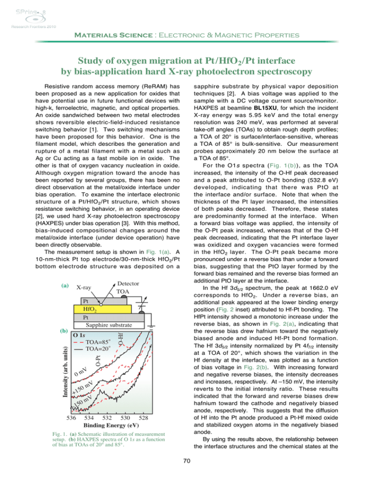
Materials Science : Electronic & Magnetic Properties Study of oxygen migration at Pt /HfO2 /Pt interface by bias-application hard X-ray photoelectron spectroscopy sapphire substrate by physical vapor deposition techniques [2]. A bias voltage was applied to the sample with a DC voltage current source/monitor. HAXPES at beamline BL15XU, for which the incident X-ray energy was 5.95 keV and the total energy resolution was 240 meV, was performed at several take-off angles (TOAs) to obtain rough depth profiles; a TOA of 20° is surface/interface-sensitive, whereas a TOA of 85° is bulk-sensitive. Our measurement probes approximately 20 nm below the surface at a TOA of 85°. For the O1s spectra (Fig. 1(b)), as the TOA increased, the intensity of the O-Hf peak decreased and a peak attributed to O-Pt bonding (532.8 eV) developed, indicating that there was PtO at the interface and/or surface. Note that when the thickness of the Pt layer increased, the intensities of both peaks decreased. Therefore, these states are predominantly formed at the interface. When a forward bias voltage was applied, the intensity of the O-Pt peak increased, whereas that of the O-Hf peak decreased, indicating that the Pt interface layer was oxidized and oxygen vacancies were formed in the HfO 2 layer. The O-Pt peak became more pronounced under a reverse bias than under a forward bias, suggesting that the PtO layer formed by the forward bias remained and the reverse bias formed an additional PtO layer at the interface. In the Hf 3d5/2 spectrum, the peak at 1662.0 eV corresponds to HfO 2 . Under a reverse bias, an additional peak appeared at the lower binding energy position (Fig. 2 inset) attributed to Hf-Pt bonding. The HfPt intensity showed a monotonic increase under the reverse bias, as shown in Fig. 2(a), indicating that the reverse bias drew hafnium toward the negatively biased anode and induced Hf-Pt bond formation. The Hf 3d5/2 intensity normalized by Pt 4f7/2 intensity at a TOA of 20°, which shows the variation in the Hf density at the interface, was plotted as a function of bias voltage in Fig. 2(b). With increasing forward and negative reverse biases, the intensity decreases and increases, respectively. At –150 mV, the intensity reverts to the initial intensity ratio. These results indicated that the forward and reverse biases drew hafnium toward the cathode and negatively biased anode, respectively. This suggests that the diffusion of Hf into the Pt anode produced a Pt-Hf mixed oxide and stabilized oxygen atoms in the negatively biased anode. By using the results above, the relationship between the interface structures and the chemical states at the Resistive random access memory (ReRAM) has been proposed as a new application for oxides that have potential use in future functional devices with high-k, ferroelectric, magnetic, and optical properties. An oxide sandwiched between two metal electrodes shows reversible electric-field-induced resistance switching behavior [1]. Two switching mechanisms have been proposed for this behavior. One is the filament model, which describes the generation and rupture of a metal filament with a metal such as Ag or Cu acting as a fast mobile ion in oxide. The other is that of oxygen vacancy nucleation in oxide. Although oxygen migration toward the anode has been reported by several groups, there has been no direct observation at the metal/oxide interface under bias operation. To examine the interface electronic structure of a Pt/HfO 2 /Pt structure, which shows resistance switching behavior, in an operating device [2], we used hard X-ray photoelectron spectroscopy (HAXPES) under bias operation [3]. With this method, bias-induced compositional changes around the metal/oxide interface (under device operation) have been directly observable. The measurement setup is shown in Fig. 1(a). A 10-nm-thick Pt top electrode/30-nm-thick HfO 2 /Pt bottom electrode structure was deposited on a (a) Detector TOA X-ray Pt HfO2 TOA=85◦ TOA=20◦ V 0m 50 +1 O-Hf O 1s O-Pt Intensity (arb. units) (b) Pt Sapphire substrate mV V 0m 5 1 - 536 534 532 530 528 Binding Energy (eV) Fig. 1. (a) Schematic illustration of measurement setup. (b) HAXPES spectra of O 1s as a function of bias at TOAs of 20° and 85°. 70 Intensity (arb. unit) Relative Intensity HfPt (kcps) (a) 1.2 0.8 0.4 Hf 3d5/2 exp. sum. HfO2 HfPt 1666 1662 1658 Binding Energy (eV) 0.0 (b) Relative Intensity Hf 3 d5/2 (kcps) 50 45 40 -150 -100 -50 0 50 100 150 Applied Voltage (mV) 35 Fig. 2. Applied bias dependences of (a) Hf 3d5/2 intensity ratio of HfPt (squares) and (b) intensity of Hf 3d5/2 (triangles). All spectra were normalized by the Pt 4f intensity of Pt at 0 V (initial state). The inset shows HAXPES spectra of Hf 3d5/2 at a bias of –150 mV (reverse bias) and a TOA of 20°. The solid line and open circles show the spectra and sum-fitted curve, respectively. Dashed lines are fitted curves for HfO2 and HfPt bonds. the biases were smaller than the threshold voltage at which the high resistance state changes to a low resistance state; therefore, our results did not describe the resistance-changing behavior. However, the most important implication of our results is that oxygen migration occurs at low bias voltages. The control of oxygen migration and the oxidization of the interface between metal and oxide have the potential to become key techniques for exploiting the electrical properties of metals on oxides. Pt/HfO2/Pt interface under different biases is summarized as Fig. 3. The application of a forward bias causes oxygen to diffuse into the Pt layer, forming PtO (Fig. 3(b)). Under a reverse bias (Fig. 2(c)), the PtO layer remains at the interface, whereas hafnium moves to the interface, forming additional Pt-O and Pt-Hf bonds. Note that this oxygen vacancy formation behavior is consistent with the reported electrical properties, namely, oxygen vacancies form percolating conduction filaments during ReRAM applications. In this study, (a) Initial state (b) Forward bias (c) Reverse bias Pt (anode) +++++++++++ Pt (anode) - - - - - - - - - - - Pt-O Pt-O Pt Pt Pt-O Pt | O O O O | | HfO2 Pt | Hf O O HfO2 Pt Pt Pt | | | O O O Pt (anode) Hf O O - - - - - - - - - - - HfO2 O O | | Pt Pt Hf Pt Hf | | | | | O Hf Pt Hf Pt Hf Hf Hf +++++++++++ Fig. 3. Schematic illustration of Pt/HfO 2 interfaces at (a) initial state and under (b) forward and (c) reverse biases. References [1] M. Haemori et al.: Appl. Phys. Express 2 (2009) 061401. [2] T. Nagata, M. Haemori, Y. Yamashita, H. Yoshikawa, Y. Iwashita, K. Kobayashi and T. Chikyow: Appl. Phys. Lett. 97 (2010) 082902. [3] Y. Yamashita et al.: e-J. Surf. Sci. Nanotech. 8 (2010) 81. Takahiro Nagata a,*, Yoshiyuki Yamashita a,b and Keisuke Kobayashi b a Advanced Electric Materials Center, National Institute for Materials Science b NIMS Beamline Station at SPring-8, National Institute for Materials Science *E-mail: NAGATA.Takahiro@nims.go.jp 71

