Ultra High Speed Digital Processing for Wireless
advertisement
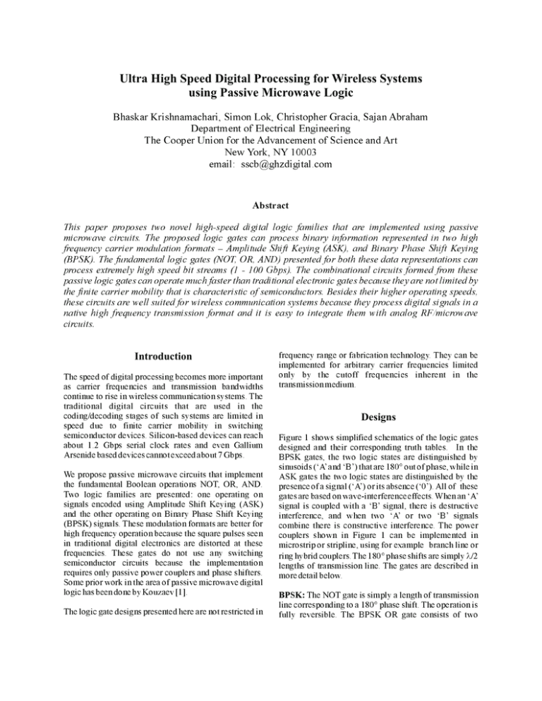
Ultra High Speed Digital Processing for Wireless Systems using Passive Microwave Logic Bhaskar Krishnamachari, Simon Lok, Christopher Gracia, Sajan Abraham Department of Electrical Engineering The Cooper Union for the Advancement of Science and Art New York, NY 10003 email: sscb@ghzdigital.com Abstract This paper proposes two novel high-speed digital logic families that are implemented using passive microwave circuits. The proposed logic gates can process binary information represented in two high frequency carrier modulation formats Amplitude Shift Keying (ASK), and Binary Phase Shift Keying (BPSK). The fundamental logic gates (NOT, OR, AND) presented for both these data representations can process extremely high speed bit streams (1 - 100 Gbps). The combinational circuits formed from these passive logic gates can operate much faster than traditional electronic gates because they are not limited by the finite carrier mobility that is characteristic of semiconductors. Besides their higher operating speeds, these circuits are well suited for wireless communication systems because they process digital signals in a native high frequency transmission format and it is easy to integrate them with analog RF/microwave circuits. frequency range or fabrication technology. They can be Introduction implemented for arbitrary carrier frequencies limited The speed of digital processing becomes more important only as carrier frequencies and transmission bandwidths transmission medium. by the cutoff frequencies inherent in the continue to rise in wireless communication systems. The traditional digital circuits that are used in the coding/decoding stages of such systems are limited in speed due to finite carrier mobility in Designs switching semiconductor devices. Silicon-based devices can reach Figure 1 shows simplified schematics of the logic gates about 1.2 Gbps serial clock rates and even Gallium designed and their corresponding truth tables. Arsenide based devices cannot exceed about 7 Gbps. BPSK gates, the two logic states are distinguished by In the sinusoids (A and B) that are 180° out of phase, while in We propose passive microwave circuits that implement ASK gates the two logic states are distinguished by the the fundamental Boolean operations NOT, OR, AND. presence of a signal (A) or its absence (0). All of these Two logic families are presented: one operating on gates are based on wave-interference effects. When an A signals encoded using Amplitude Shift Keying (ASK) signal is coupled with a B signal, there is destructive and the other operating on Binary Phase Shift Keying interference, and when two A or two B signals (BPSK) signals. These modulation formats are better for combine there is constructive interference. The power high frequency operation because the square pulses seen couplers shown in Figure 1 can be implemented in in traditional digital electronics are distorted at these microstrip or stripline, using for example branch line or frequencies. These gates do not use any switching ring hybrid couplers. The 180° phase shifts are simply l/2 semiconductor circuits because the implementation requires only passive power couplers and phase shifters. Some prior work in the area of passive microwave digital logic has been done by Kouzaev [1]. The logic gate designs presented here are not restricted in lengths of transmission line. The gates are described in more detail below. BPSK: The NOT gate is simply a length of transmission line corresponding to a 180° phase shift. The operation is fully reversible. The BPSK OR gate consists of two NOT P S K A S K Input OR Input 1 180° Shift Output `B’ Signal Generator AND Power Coupler Input 2 B A A B Input `B’ Signal Generator Power Coupler 180° Shift 0 A A 0 Power Coupler A A B B A B A B Power Coupler Input 1 Power Coupler Output `A’ Signal Generator A B B B A A B B Input 2 A B A B Output A A A B Signal Key Input 1 Power Coupler `A’ Signal Output Output 0 0 A A Input 2 0 A 0 A `B’ Signal 0 A A A `0’ Signal Figure 1: GHz Digital Logic Gate Designs couplers. If input 1 is A, it destructively combines with the worst case half of the power is lost in each gate due to the B signal at the first coupler so that the output of the this first coupler is always 0 which makes the output of the (IDSSD). The energy required for the operations is gate the same as input 2. If input 1 is B then it obtained directly from the signals being processed (as constructively combines with the B signal from the power dissipation during destructive interference). In the generator at the first coupler to generate a B signal with implementation of these gates, significant power losses twice the power as the output of the first coupler. In this are a tradeoff for high speed performance. input-dependent systemic signal degradation case the output of the gate will be B independent of the state of input 2. As can be seen from the designs, the One of the advantages of active digital logic over passive BPSK AND gate is very similar in operation and is a logic is that traditional digital electronic signals are dual of the OR gate. regenerated after each gate. There are amplitude variations in the outputs of the passive gates (which can ASK: In the ASK NOT gate, the input is coupled to a B affect performance, particularly in ASK circuits where signal generator and the output of the coupler is phase amplitude level discrimination becomes an issue) and shifted by 180°. If the input is a 0 signal, the output of the phase variations that will be introduced due to fabrication coupler is a B signal which then becomes an A signal errors at these high frequencies. To combat the effect of because of the phase shift. If the input is an A signal, the IDSSD and other variations, active regenerating destructive interference takes place and the output of the limiter/amplifier blocks may be needed after four or five coupler is 0 signal which undergoes no change in the cascaded stages of passive logic gates. These active phase shifter and emerges as the output of the gate. The regenerators ASK OR gate is simply a power coupler. The output is a microwave analog devices that are capable of operating at 0 only if no inputs are presented to the gate and an A extremely high frequencies. can be designed to utilize existing signal if one or both inputs is an A signal. The coupler blocks shown in Figure 1 seem to be three port devices, but all passive microwave couplers are four port networks. There is dissipation of power if only one input presented to a coupler. This results in the signals attenuating as they propagate through cascaded gates. In Simulation Results These circuit designs have been extensively simulated over a wide range of frequencies for implementation in Input 1 microstrip and stripline. Some ASK gates have been fabricated, tested and demonstrated previously at 300 Mhz [2]. We are currently working on fabricating and testing higher frequency circuits for both ASK and BPSK. The results shown in this paper are for 10 GHz stripline circuits with a 20-mil ground plane spacing in a dielectric with er of 9.9. The software used for design and simulation was the HP EEsof Series IV Communication Design Suite. Figure 2 shows simulation results demonstrating the operation of a BPSK AND gate for a carrier frequency of 10 GHz. Five cycles of the carrier wave are chosen to represent one bit, so the circuit operating bit rate is 2 Gbps. The output of the OR/AND gate lags the input changes by one and one quarter carrier cycles. This is due to the physical dimensions of the circuit (5/4 l) Input 2 and represents the time delay or latency of the BPSK gates. Figures 3 and 4 show simulation results for the ASK OR and NOT gates implemented in stripline for a carrier frequency of 10 GHz. The bit rate is again a fifth of the carrier, 2 Gbps. The output in these gates shows a time delay of half a cycle corresponding to the circuit dimensions (l/2). Conclusions Designs for two novel high-speed digital logic families utilizing passive microwave circuits operating on binary information modulated using ASK and BPSK schemes have been presented. Simulations confirming the designs Output (with A signal reference) for operating speeds of 2 Gbps have also been shown. There is room for significant further work in this field, particularly with regard to developing functioning multigate combinational circuits, and compatible memory devices. These logic families have a great potential for application in wireless communication systems because of their high operating speeds, processing of data in high frequency transmission formats and ease of integration with analog microwave circuitry. Acknowledgements Dr. Toby Cumberbatch, Associate Professor of Electrical Engineering at The Cooper Union, for his guidance and advice. Dr. Aly Fathy of Sarnoff Corporation for giving us the foundations of our knowledge in microwave engineering. Figure 2: Simulated PSK AND Gate Results (10 GHz, 2 Gbps) Input ( Input 1 Input 2 Output ( ) ) Figure 4: Simulated ASK NOT Gate Results (10 GHz, 2 Gbps) References [1] Kouzaev, G.A.; Gvozdev, V.I. Topological pulsemodulation of field and new microwave circuits design for superspeed operating device, International Symposium on Signals, 1995 URSI Systems and Electronics, pp. 383-384 Output [2] Abraham S., Gracia, C. Krishnamachari B., Lok S. 300 MHz ASK digital logic gates in microstrip, IEEE Sarnoff Symposium on Advances in Wired and Wireless Communications, March 1998, pp. 173-175 Figure 3: Simulated ASK OR Gate Results (10 GHz, 2 Gbps)
