Large Signal Bias Dependent Modeling of Avalanche Photodiode
advertisement
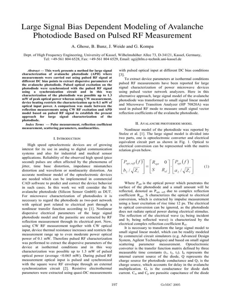
Large Signal Bias Dependent Modeling of Avalanche Photodiode Based on Pulsed RF Measurement A. Ghose, B. Bunz, J. Weide and G. Kompa Dept. of High Frequency Engineering, University of Kassel, Wilhelmshöher Allee 73, D-34121, Kassel, Germany, Tel: +49-561 804 6528, Fax: +49-561 804 6529, Email: ag@hfm.e-technik.uni-kassel.de Abstract — This work presents a method for large signal characterization of avalanche photodiode (APD) where measurements were carried out using pulsed RF signal at different DC bias points to extract dispersive parameters of the avalanche photodiode. Pulsed optical excitation on the photodiode were synchronized with the pulsed RF signal using a synchronization circuit and in this way characterization of the photodiode was possible up to 1.3 mW of peak optical power whereas using CW measurement, device heating restricts the characterization up to 0.1 mW of optical input power. A comparison was made between the reflection measurements using CW RF excitation and APD model based on pulsed RF signal to establish the present approach for large signal characterization of the photodiode. Index Terms — Pulse measurement, reflection coefficient measurement, scattering parameters, nonlinearities. I. INTRODUCTION High speed optoelectronic devices are of growing interest for its use in analog to digital communication systems and also for industrial and medical sensor applications. Reliability of the observed high speed (pico second) pulses are often affected by the phenomena of jitter, time base distortion, impedance mismatches distortion and waveform or nonlinearity distortion. An accurate nonlinear model of the optoelectronic devices are needed which can be implemented in commercial CAD software to predict and correct the device behavior in such cases. In this work we will consider the Si avalanche photodiode (Silicon Sensor GmbH) as DUT. For microwave characterization of photodiodes it is necessary to regard the photodiode as two-port network with optical port related to electrical port through a nonlinear transfer function according to [1]. Nonlinear dispersive electrical parameters of the large signal photodiode model and the parasitic are extracted by RF reflection measurement through its electrical port. Now, using CW RF measurement together with CW optical input, device thermal resistance increases and restricts the measurement range up to even moderate power optical power of 0.1 mW. Therefore pulsed RF characterization was performed to extract the dispersive parameters of the device at isothermal conditions and in this way characterization was possible up to 1.3 mW of pulsed optical power (average <0.065 mW). During pulsed RF measurement optical input is pulsed and synchronized with the square wave RF envelope through an external synchronization circuit [2]. Resistive electrothermal parameters were extracted using quasi-DC measurements 197 with pulsed optical input at different DC bias conditions [3]. To extract device parameters at isothermal conditions pulsed RF measurements have been reported for large signal characterization of power microwave devices using pulsed vector network analyzers. Here in this alternative approach, large signal model of the avalanche photodiode was transformed to small signal linear model and Microwave Transition Analyzer (HP 70820A) was used in pulsed RF mode to measure small signal vector reflection coefficients of the avalanche photodiode. II. AVALANCHE PHOTODIODE MODEL Nonlinear model of the photodiode was reported by Stolze et al. [1]. The large signal model is divided into two parts, one is optoelectronic converter and electrical equivalent circuit part as shown in Fig. 1. Optical to electrical conversion can be represented with the matrix relation given below. Where Popt is the optical power which penetrates the surface of the photodiode and a small amount will be reflected, denoted as Popt, refl due to complex reflection coefficient Ropt. S characterizes the optical to electrical conversion, which is extracted by impulse measurement using a laser excitation of rise time 12 ps. The electrical to optical conversion can be ignored, as the photodiode does not radiate optical power during electrical stimulus. The reflection of the electrical wave (a2 being incident and b2 being reflected wave) is characterized by the electrical complex reflection coefficient Rel. It is necessary to transform the large signal model to small signal linear model, which can be readily modeled by commercial circuit simulators (e.g. Advanced Design System, Agilent Technologies) and based on small signal scattering parameter measurement. Optoelectronic converter is the transfer function matrix defined by three measurable time constants (t1, t2, t3). I0 represents the internal current source of the diode, Q represents the charge source for photodiode conductance and Q1 is the charge source, which accounts for delay in the avalanche multiplication. Gr is the conductance for diode dark current. Cm and Cp are parasitic capacitance of the diode GeMiC 2005 bond pad. Rm and Lm are bond wire resistance and inductance respectively. The large signal model describes the nonlinear dependence of internal photocurrent I2 to the diode current I1 by the current source I0 and charge source Q. Rs being the internal series resistance of the photodiode is a nonlinear element dependent on I2 and V2. In Fig. 2 linearized photodiode model is shown with charge sources replaced by diode conductance G0 and diode capacitance C0. Delay charge source is represented by time constant of the series R1 and C1. Control current I1 is delayed by the delay coefficient tp1. Electrothermal parameters were measured by quasi-DC I-V characteristic of the diode and dispersive parameters were extracted by pulsed RF measurements. Fig. 1. Large signal model of the avalanche photodiode Fig. 2. Derived small signal model of the avalanche photodiode [2] The set up was built around Microwave Transition Analyzer (HP70820A) with synthesized signal generator (HP 8360B) as shown in Fig. 4. RF pulses were provided by synthesized source through bias decouple circuit followed by a directional coupler and 23 dB attenuator to the DUT (avalanche photodiode). Reflected pulses were coupled from the forward RF signal by the directional coupler (3 dB). Low frequency components of the electrical pulse from the photodiode (5 micro second pulse width, 5 kHz PRF) were filtered by the bias decoupling circuit. Pulsed RF measurement was carried out from 1 GHz to 30 GHz. Synthesized sweeper was controlled by Microwave Transition Analyzer in the pulsed RF mode. Optical stimulus on the photodiode was synchronized with a synchronization circuit having adjustable amplitude, pulse width and delay. TTL pulses from the Microwave Transition Analyzer trigger the input of the synchronization circuit and output pulses from the synchronization circuit drives a low noise voltage to current converter (LDX3620) for the laser diode (LQ6780-4a/OECA). Optical power was measured at the output of the optical fiber. Establishment of the measurement point over the pulse is done by placing the microwave transition analyzer in time sweep mode and then a time delay is set between the trigger point (leading edge of the pulse) and measurement point. Measurement point was set near the end of the pulse to avoid overshoot of the pulse [5]. The vector reflection measurement of the device at a specific input pulsed RF power yields a set of raw measurement vectors. S parameters of the directional coupler were measured separately using a HP8510 vector network analyzer and vector error correction was done of the measured reflection coefficients. 10 MHz Ref. III. MEASUREMENT TECHNIQUE Input MOD Output HP IB In Fig. 3 Schematic of the principle of the used pulsed RF measurement is shown. Optical pulses are synchronized with the pulse envelope of the RF excitation. A safe limit of about 1 micro second was left to perform the measurement at relatively ripple free region of the pulse. CH1 Out RF Source Power Splitter CH2 Microwave Transition Analyser (+/- 2 V or 16 dBm Tol.) RF Out 11 dBm (0 V or 0.5 Watt Tol.) 20 dB 6 dB Bias supply 3 dB 23 dB 2 mV peak (measured) DUT (APD) Bias decouple Directional Coupler Blocking Cap. 3 dB 0.15 V peak +5 V Sync. Circuit Current source Laser diode Fig. 4. Set up for pulsed RF characterization Fig. 3. Pulsed (RF and opt.) measurement principle 198 GeMiC 2005 OP. Fibre IV. EXTRACTED PARAMETERS Intrinsic parameters of the photodiode were extracted after de-embedding the extrinsic parameters Lm and Cp from the measured Y parameters. Extrinsic parameters are bias independent and also independent of optical power. Fig. 7. Extracted Q from pulsed RF measurement Fig. 5. Measured photodiode capacitance using pulsed RF signal and its variation with optical power and bias voltage Lm is found to be 276 nH and Cp, the pad capacitance is 0.020 pF. Fig. 5 shows the extracted nonlinear diode capacitance with change in bias voltage and optical conditions using above method of pulsed RF measurement. From Fig. 5, it is evident that the diode capacitance is nearly 2 pF over the bias region of 50 Volt to 148 Volt and a slight decrease to 1 pF is noticed at optical power higher than 1 mW. This is because of increased diode conductance at the reverse bias in the breakdown region (measured breakdown voltage 148.5 V) and optical power of more than 1 mW. In Fig. 7, charge stored at the depletion region of the photodiode is plotted with photodiode bias and optical power input. Charge stored in the depletion region increases steadily with increase in optical power and bias voltage. Slight variation is noticed at break down region of more than 100 volt due to variation of capacitance at that region (Fig. 5). Fig. 8a. Magnitude of measured (triangle) reflection coefficient using Vector Network Analyzer (HP 8510) and modeled (solid) based on pulsed RF measurement Fig. 6. Measured (pulsed RF) diode conductance Fig. 6, [1/g0]RF (diode conductance: g0) shows slight monotonous variation at the bias region of 50 Volt to 100 Volt and rapid decrease is noticed with optical power input of more than 1 mW. This indicates a decreased gain and simultaneously increased thermal resistance of the device [3]. 199 Fig. 8b. Measured phase response of reflection coefficients using Vector Network Analyzer (HP 8510) (triangle) and modeled (solid) based on pulsed RF measurement GeMiC 2005 Fig. 8a and Fig. 8b shows the comparison of measured reflection coefficient using Vector Network Analyzer (HP 8510) [4] and modeled photodiode based on pulsed RF measurement at the similar optical conditions. Slight deviation (Fig. 8a) is observed after 28 GHz due to increased loss at the bias network. V. CONCLUSION It was confirmed that the pulsed RF measurement, which is generally used for power microwave devices to measure low frequency dispersion etc. can also be used for optoelectronic devices like avalanche photodiode to characterize optical power dependent nonlinearities of the photodiode. Avalanche gain is very sensitive to device temperature, therefore present approach allows near isothermal characterization of the device. It was possible to characterize the device up to 1.3 mW of peak optical power, which covers the dynamics of the signal at which it is exposed in practical use e.g. pulsed laser radar system. Photodiode model was implemented by a harmonic balance simulator and modeled reflection coefficients were compared with standard reflection measurement using CW RF signal by Vector Network Analyzer for confirmation at the low optical power level. ACKNOWLEDGEMENT This work was performed within the European research project (INTAS 51615009). Financial support is greatly acknowledged. REFERENCES [1] Stolze, A., and Kompa, G., “Nonlinear modeling of dispersive photodiodes based on frequency and timedomain measurements”, 26th European microwave conference. Proc., Prague, Czech Republ., pp. 379382, September 9-12, 1996. [2] Ghose, A., Bunz, B., Weide, J., and Kompa, G., “Measurement of nonlinear dispersive parameters of avalanche photodiode using pulsed RF signal and quasi-DC optical stimulus,” 34th European Microwave Conf., Proc., Amsterdam, The Netherlands, pp. 925-928, November 11-15, 2004. [3] Ghose, A., and Kompa, G., “Electrothermal parameter extraction of avalanche photodiode using quasi-DC optical pulses,” 10th IEEE International Symposium on Electron Devices for Microwave and Optoelectronic Applications, Proc., Manchester, UK, pp. 69-74, November 18-19, 2002. [4] Ghose, A., Ring, M, and Kompa, G., “Simultaneous gain and noise matching of a wideband optical receiver front end,” 2003 Asia Pacific Microwave Conference, Proc., Seoul Korea, pp. 431-434, November 4-7, 2003. [5] Baylis, C. P., and Dunleavy, L. P., “Performing and analyzing pulsed current-voltage measurements,” High Frequency Electronics, pp. 64-69, May 2004. 200 GeMiC 2005
