A Deep Silicon Via (DSV) Ground for SiGe Power
advertisement

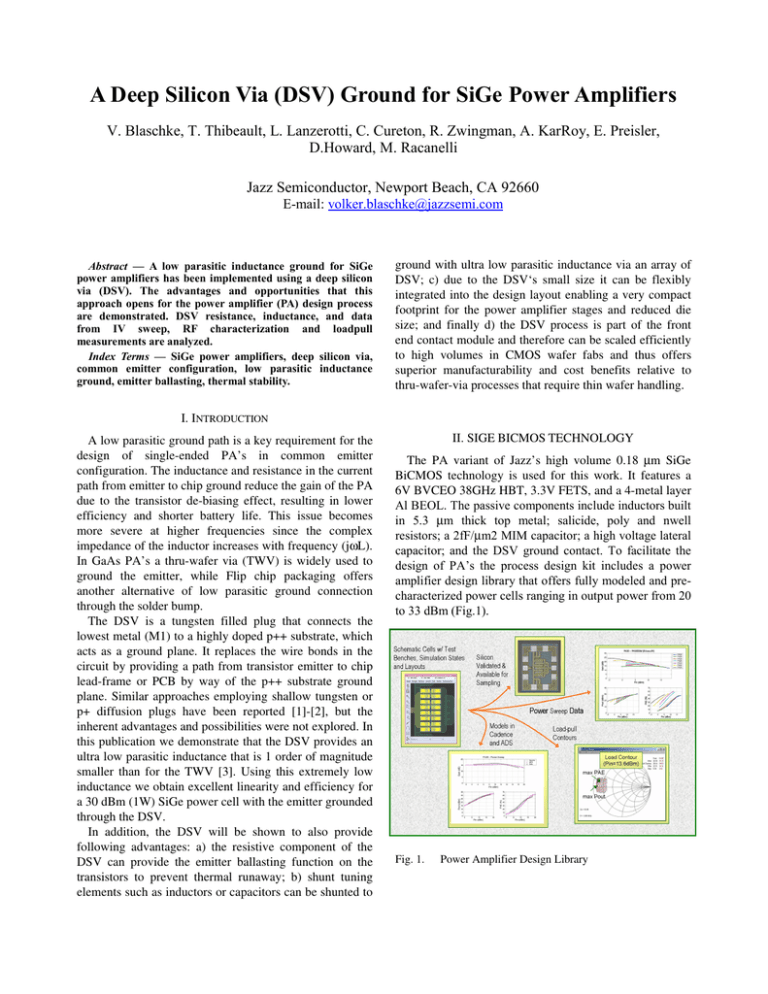
A Deep Silicon Via (DSV) Ground for SiGe Power Amplifiers V. Blaschke, T. Thibeault, L. Lanzerotti, C. Cureton, R. Zwingman, A. KarRoy, E. Preisler, D.Howard, M. Racanelli Jazz Semiconductor, Newport Beach, CA 92660 E-mail: volker.blaschke@jazzsemi.com Abstract — A low parasitic inductance ground for SiGe power amplifiers has been implemented using a deep silicon via (DSV). The advantages and opportunities that this approach opens for the power amplifier (PA) design process are demonstrated. DSV resistance, inductance, and data from IV sweep, RF characterization and loadpull measurements are analyzed. Index Terms — SiGe power amplifiers, deep silicon via, common emitter configuration, low parasitic inductance ground, emitter ballasting, thermal stability. ground with ultra low parasitic inductance via an array of DSV; c) due to the DSV‘s small size it can be flexibly integrated into the design layout enabling a very compact footprint for the power amplifier stages and reduced die size; and finally d) the DSV process is part of the front end contact module and therefore can be scaled efficiently to high volumes in CMOS wafer fabs and thus offers superior manufacturability and cost benefits relative to thru-wafer-via processes that require thin wafer handling. I. INTRODUCTION A low parasitic ground path is a key requirement for the design of single-ended PA’s in common emitter configuration. The inductance and resistance in the current path from emitter to chip ground reduce the gain of the PA due to the transistor de-biasing effect, resulting in lower efficiency and shorter battery life. This issue becomes more severe at higher frequencies since the complex impedance of the inductor increases with frequency (jωL). In GaAs PA’s a thru-wafer via (TWV) is widely used to ground the emitter, while Flip chip packaging offers another alternative of low parasitic ground connection through the solder bump. The DSV is a tungsten filled plug that connects the lowest metal (M1) to a highly doped p++ substrate, which acts as a ground plane. It replaces the wire bonds in the circuit by providing a path from transistor emitter to chip lead-frame or PCB by way of the p++ substrate ground plane. Similar approaches employing shallow tungsten or p+ diffusion plugs have been reported [1]-[2], but the inherent advantages and possibilities were not explored. In this publication we demonstrate that the DSV provides an ultra low parasitic inductance that is 1 order of magnitude smaller than for the TWV [3]. Using this extremely low inductance we obtain excellent linearity and efficiency for a 30 dBm (1W) SiGe power cell with the emitter grounded through the DSV. In addition, the DSV will be shown to also provide following advantages: a) the resistive component of the DSV can provide the emitter ballasting function on the transistors to prevent thermal runaway; b) shunt tuning elements such as inductors or capacitors can be shunted to II. SIGE BICMOS TECHNOLOGY The PA variant of Jazz’s high volume 0.18 μm SiGe BiCMOS technology is used for this work. It features a 6V BVCEO 38GHz HBT, 3.3V FETS, and a 4-metal layer Al BEOL. The passive components include inductors built in 5.3 μm thick top metal; salicide, poly and nwell resistors; a 2fF/μm2 MIM capacitor; a high voltage lateral capacitor; and the DSV ground contact. To facilitate the design of PA’s the process design kit includes a power amplifier design library that offers fully modeled and precharacterized power cells ranging in output power from 20 to 33 dBm (Fig.1). Fig. 1. Power Amplifier Design Library III. DEEP SILICON VIA CHARACTERIZATION The DC resistance of a single DSV was obtained using measurements on a Kelvin test structure that connects 2 DSV in series with the chain link being the p++ substrate. Half the measured value represents the tungsten plug, metal to silicon interface and spreading resistance through the substrate. A single DSV has a nominal resistance of 51Ω (Fig.2). 60 T50=51.1 Ω resonance frequency of a shunt resonator. The shunt resonator branch consists of a capacitor that is grounded through an array of 9x9 DSV. The inductance results in table 1 show that the DSV inductance of 2-2.5 pH is ~1 order of magnitude smaller than the TWV inductance [3]. TABLE I. EXTRACTED INDUCTANCE Ground Method Measurement Approach Inductance 1 DSV 81 DSV TWV [3] Direct (Single Port) Shunt Resonator Shunt Resonator 2.5 pH 2.0 pH 21.3 pH 50 The impedance to ground is mainly resistive (Re). With the large collector current (Ic) in a power amplifier cell, the 2. power dissipation in the resistor (Ic Re) becomes significant and a large number of DSV’s is required to minimize Re. Count 40 30 20 10 IV. DSV APPLICATION EXAMPLES 0 30 35 40 45 50 55 Resistance (Ω) 60 65 70 Fig. 2. DC Resistance of DSV The inductance was extracted from S-parameters using 2 different on-wafer test approaches. A single port test structure was used to directly extract the inductance for a single via. The DSV is connected to the signal probe pad with microstrip lines of various lengths. By extrapolating the measured value of inductance over the length of the microstrip feeds, the inductance of the DSV is obtained from the y-intercept when the length of the microstrip is zero (Fig. 3). Silicon with a thermal conductivity 3 times better than GaAs permits very compact power cell layouts. The 30 dBm cell in Fig.4 measures 220x375 μm and was laid out using modular npn building blocks adding to a total 2 emitter area of 4608 μm and a DSV Re of 50 mΩ. The xsection in Fig.5 shows 3 rows of DSV in the immediate neighborhood of the npn block making evident the short path from the transistor emitter to ground. 80 70 60 L (pH) 50 40 30 Fig. 4. Power cell 30 dBm Fig. 5. NPN Emitter ground with DSV y−intercept = 2.5 pH L model = 5.0 pH 20 10 0 0 Fig. 3. 50 100 150 200 250 Launcher Length (um) 300 350 Inductance of single DSV A two port test structure in T-network configuration was used to indirectly extract the inductance from the 1dB compression points for large signal power sweep measurements are marked on the curve and are located well below the region where thermal instability occurs. However in large arrays of transistors, the center of the array can become sufficiently hot and since the current increases with temperature for SiGe HBT’s, more charge flows to the hot transistor leading to thermal runaway. 3 10 Vce=3.0V Vce=3.3V Vce=3.5V Vce=3.8V Vce=4.0V 2 Collector Current (mA) Since large arrays of npn’s have very small input impedances on the order of 2 Ω or less, matching this impedance requires very small inductances on the order of a few hundred pH in combination with a large shunt capacitance. Any parasitic inductance in routing the shunt capacitor to ground will detune this matching network. The DSV process supports stacking the mimcap on top of a DSV array (Fig. 6). Layout splits on different densities of DSV and via1 to connect the bottom plate of the capacitor show that the integrity of the mimcap is not disturbed (Fig. 7). 10 1 10 P1dB Bias DC Bias 0 10 −1 10 0.7 0.72 0.74 0.76 0.78 0.8 Base−Emitter Bias (V) 0.82 0.84 0.86 Fig. 8. IV-Sweep on 6V npn, 72μm2 emitter area Fig. 6. Shunt mimcap ground with DSV A comparison of IV-sweeps on 30 dBm power cells 2 with an emitter area of 4608 μm and different ballasting options show that the cells using a base ballast resistor and or cells grounded through the DSV withstand the IVsweep, while the cell without ballast resistor or DSV fails (Fig. 9). 35 BVGo (V) 30 25 20 Fig. 7. 1: DSV=1x, Via1=0 2: DSV=2x, Via1=0 3: DSV=1x, Via1=1x 4: DSV=2x, Via1=1x 5: DSV=1x, Via1=4x 6: DSV=2x, Via1=4x 1 2 3 4 Split Group 5 6 Breakdown voltage of 22pH shunt mimcap Collector Current (mA) 800 Breakdown 700 600 500 400 300 Rb=0, Re=0 Rb=96Ω, Re=0 Rb=0, Re=DSV *) Rb=96Ω, Re=DSV *) Extracted *) − ΔVe 200 100 V. EMITTER BALLASTING Although silicon has a very good thermal conductivity it is still necessary to protect SiGe PA’s from thermal destruction. The IV-sweep on a 6V npn with emitter area 2 72 μm demonstrates that SiGe HBT’s can be driven into thermal instability (Fig. 8). The collector current initially rises as expected from the turn-on action of the pnjunction until the increase in power dissipation and junction temperature cause the curve to bend upwards pushing the device into thermal instability. DC Bias and 0 0.75 0.8 0.85 Base−Emitter Bias (V) 0.9 Fig. 9. IV-Sweep on 30 dBm power cell with various ballasting options The curves for the power cells with DSV can be extrapolated to close agreement to the curves for power cells without DSV by correcting for the calculated voltage drop ΔVe over the DSV, showing that the difference in the curves is entirely due to the resistance Re. This resistive component provides a ballast resistor at the emitter. 0.16 Breakdown Jcc (mA/um2) 0.14 70 35 60 30 50 25 40 20 30 PAE (%) 0.2 0.18 40 Gain (dB) / Pout (dBm) The IV-sweep results in Fig. 10 compare a 33 dBm (2 2 W) power cell of 9216 μm emitter area using a 3 Ω salicide resistor at the emitter of each individual transistor for ballast to the 30 dBm power cell with DSV ground. 15 20 0.12 10 0.1 5 Gain (P1dB=16.1dB) Pout (P1dB=30.5dBm) PAE (P1dB=51.0%) 0.08 0 0 0.06 PA30 : Re=0 PA33 : Re=0 PA30 : Re=DSV*2 PA30 : Re=DSV*1 PA33 : Re=3Ω 0.04 0.02 0 0.75 0.8 0.85 Base−Emitter Bias (V) 2 4 6 8 10 12 14 16 18 20 10 0 Pin (dBm) Fig. 11. Power sweep result on 30 dBm cell without DSV 40 0.9 60 35 50 VI. LOADPULL POWER SWEEP The linearity and efficiency of the 30 dBm power cell was characterized using on-wafer loadpull measurements with tuning at the fundamental frequency of 1.88 GHz. For the non-ballasted power cell, strong gain expansion is evident (Fig. 11). The power cell with DSV exhibits much better gain linearity and a slightly higher efficiency since it compresses later (Fig. 12). The difference in gain to the cell without DSV, at the small signal level prior to where gain expansion is observed, is 0.6 dB. Considering that this results is for the double length path for the emitter current, the reduction in gain due to Re is very small. 40 25 20 30 PAE (%) Without any ballast both cells fail as the current density increases due to thermal runaway. With emitter ballast either through discrete salicide resistors or DSV ground, the cells do not fail. The layout with the DSV employs a double length path for the emitter current to sink into the substrate and then be routed up to the top metal ground probe. This approach was used to enable quick turnaround wafer level measurements, while in a circuit application the emitter current would see only half of that path. By correcting for half of the voltage drop 0.5*ΔVe, the IV-curve of the 30 dBm power cell is close to the result of the 33 dBm resistor ballasted power cell. Hence the distributed nature of the resistance of a large array of DSV provides an emitter ballasting function similar to discrete salicide resistors. 30 Gain (dB) / Pout (dBm) Fig. 10. IV-Sweep on 30 dBm and 33 dBm power cells with DSV and discrete resistor emitter ballasting 15 20 10 10 5 0 0 Gain (P1dB=13.3dB) Pout (P1dB=30.0dBm) PAE (P1dB=53.3%) 2 4 6 8 10 12 14 16 18 0 20 Pin (dBm) Fig. 12. Power sweep result on 30 dBm cell with DSV VII. CONCLUSION The DSV ground is a very attractive option for SiGe PA’s due to the small size, low parasitic inductance and manufacturing cost benefits. Various applications such as shunt connection of mimcaps and a novel implementation of emitter ballasting are demonstrated. Excellent linearity and efficiency are obtained on large power cells. REFERENCES [1] T.Johansson, “Wireless-Trench Technology for Portable Wireless Applications,” Ericson Review, vol.1, pp.6-9, 2001. [2] W.Bakalski et al, “Design of a Dual-Band Wireless LAN SiGe-Bipolar Power Amplifier,” High Frequency Electronics, pp.18-28, Issue Sep.2004. [3] R.Uscola, M.Tutt, “Determining the Inductance of a Through-Substrate Via Using Multiple On-Wafer Test Approaches,” ICMTS Proceedings, pp.147-151, Mar. 2001.


