A Low Phase Noise Ka-Band Voltage Controlled Oscillator Using
advertisement
A Low Phase Noise Ka-Band Voltage Controlled
Oscillator Using 0.15 μm GaAs pHEMT Technology
H. L. Kao*, S. P. Shih, C. S. Yeh
L. C. Chang
Department of Electronic Engineering
Chang Gung University
Tao-Yuan, Taiwan
*snoopy@mail.cgu.edu.tw
Dept. of Materials Engineering
Ming Chi University of Technology
Taipei, Taiwan
Abstract—A low phase noise, low dissipated power and small
sized Ka-band voltage-controlled oscillator (VCO), using dual
cross-coupled pair configuration and capacitance-splitting
technique is presented. The Ka-band VCO circuit uses 0.15 μm
GaAs pHEMT technology. The VCO has low phase noise, of 116.36 dBc/Hz, at a 1 MHz offset and can be tuned from 30.5 to
31.22 GHz. The figure of merit (FOM) is -192.36 dBc/Hz. The
power consumption of the VCO with 1.04 mm2 chip area was 24
mW, from a 1 V power supply.
Keywords- phase noise, GaAs pHEMT, voltage controlled
oscillators (VCOs
I.
INTRODUCTION
GaAs pHEMT technology is the most suitable for MMW
frequencies, for System-on-Chip (SOC), due to its low noise,
high cutoff frequencies and the good linearity of GaAs pHEMT
devices. The voltage-controlled oscillator (VCO) is an
important element of a wireless transceiver/receiver. The
advantages of VCO circuits include their high frequency of
operation, low phase noise degradation, low power
consumption, wide frequency range and small die size. Many
papers have reported HEMT VCO circuits using one transistor,
for Ka-band [1], or even to W-band [2], due to high cut-off
frequency but the phase noise of HEMT-based oscillators is
higher than that of HBT-based oscillators [3]-[4] due to high
flicker noise in HEMT devices. Few reports have presented a
cross-coupled pair VCO circuit, using HBT, or HEMT
technology [5]-[6], due to the greater size and higher power
dissipation than CMOS technology [7]-[8]. However, III-V
compound semiconductor technology e.g. GaAs, InP, which
exhibits high mobility, high cut-off frequency and low loss, on
semi-insulating substrate, is suitable for millimeter-wave
(MMW) integrated circuits. 0.15 μm GaAs pseudomorphic
high electron-mobility transistor (pHEMT) technology is
selected here, because of its suitability for MMW applications,
when integrated into single-chip. In this paper, a Ka-band
VCO, using dual cross-coupled pair configuration [9] and
capacitance-splitting technique [10] is presented, to achieve
low phase noise, low power dissipation and small size. The
phase noise, at 1 MHz offset, is -116.36 dBc/Hz at 30.9 GHz,
and the tuning range is 0.72 GHz, with 24 mW power
dissipation. The chip size is 1.04 mm2. The performance of this
Ka-band VCO design compares well with the best performance
reported, in literature [1], [7]-[8].
978-1-4673-1188-5/12/$31.00 ©2012 IEEE
II.
CIRCUIT DESIGN
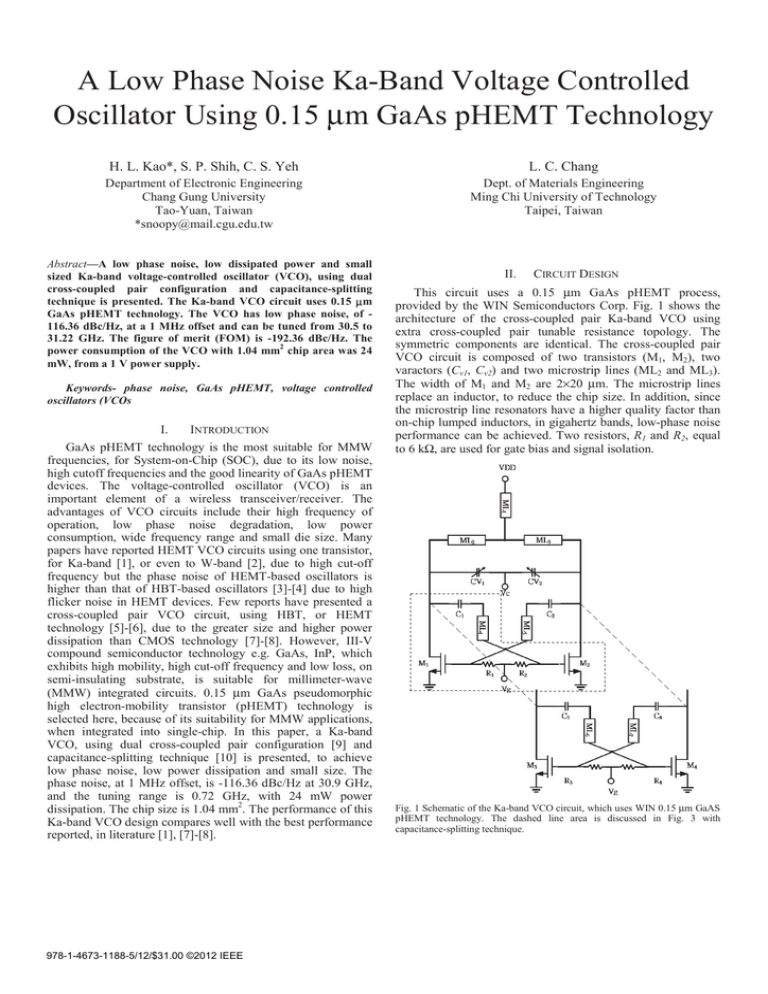
This circuit uses a 0.15 μm GaAs pHEMT process,
provided by the WIN Semiconductors Corp. Fig. 1 shows the
architecture of the cross-coupled pair Ka-band VCO using
extra cross-coupled pair tunable resistance topology. The
symmetric components are identical. The cross-coupled pair
VCO circuit is composed of two transistors (M1, M2), two
varactors (Cv1, Cv2) and two microstrip lines (ML2 and ML3).
The width of M1 and M2 are 2×20 μm. The microstrip lines
replace an inductor, to reduce the chip size. In addition, since
the microstrip line resonators have a higher quality factor than
on-chip lumped inductors, in gigahertz bands, low-phase noise
performance can be achieved. Two resistors, R1 and R2, equal
to 6 kΩ, are used for gate bias and signal isolation.
Fig. 1 Schematic of the Ka-band VCO circuit, which uses WIN 0.15 μm GaAS
pHEMT technology. The dashed line area is discussed in Fig. 3 with
capacitance-splitting technique.
A. Dual cross-coupled pair configuration
Extra cross-coupled pair tunable resistance topology is used
as the load, in the VCO circuit. Fig. 2 shows a diagram of the
proposed VCO circuit. Assuming that the gate resistance is
zero, the input impedance Zin of cross-coupled pair VCO is
Z in = −1 / g m
(1)
where gm is the transconductance of the transistor. Zin can be
tuned, by adjusting the current in transistors M3 and M4, using
the gate bias. In this work, two parallel cross-coupled pairs
were used. The width of M3 and M4 are 2×30 μm. According
to the Barkhausen criteria [11], the VCO is oscillated start-up
at
R p //( −1 / g m1, 2 ) //( −1 / g m3, 4 ) ≤ 0
(2)
where Rp denotes the passive element loss of the LC tank.
From (3)-(4), the extra cross-coupled pair topology enables the
VCO circuit to achieve the oscillator condition more easily,
due to increasing gm3,4. Transconductances, gm3,4 and gm1,2, can
be tuned by the gate bias.
It can be shown that the negative conductance was generated
by LML4, Cgs and Rg in (4):
GN =
1 − ω 2 LML 4 C gs
(1 − ω LML 4 C gs ) + (
2
2
B. Capacitance-splitting technique
The gate and drain of the cross-coupled pair are connected
by a microstrip line, ML2, in series with a DC block capacitor,
C2, which is used to improve the generating frequency of the
transistor, gm, using the capacitance-splitting technique [10].
Fig. 3 shows the equivalent circuit for a cross-coupled pair,
using the capacitance-splitting technique. The ML4 acts like an
inductor, splitting the cross-coupled pair of parasitic
capacitances, Cds of M1 and Cgs of M2. The equivalent
impedance, without considering the other parasitic effect, is
given by
Vx
=
Ix
s 2 LML 4 C gs +
sLML 4
+1
Rg
− gm
(3)
Rg
)
2
(− g m )
(4)
where Cgs and Rg are the gate to drain parasitic capacitance
and gate resistance of transistors, respectively. LML4 is the
inductance of the microstrip line. The magnitude of LML4 and
Cgs are about 10-10~10-11 H and 10-12~10-13 F, therefore, 1ω2LML4Cgs >> ωLML 4 , we can simplify (5) thus:
Rg
GN =
1
(− g m )
1 − ω LML 4 C gs
2
(5)
A larger LML4 causes larger GN. Fig. 4 shows the negative
conductance (GN=Real(1/Y22)), with and without the ML4 of
the Ka-band VCO circuit. The negative conductance generated
increases while the inductance of ML4 increases. At the
nominated operation frequency of 30.9 GHz it is increased by
a factor of 2.21. The size of transistor for the cross-coupled
pair can be reduced, for large GN, by the capacitance-splitting
technique. The power dissipation also decreases. The quality
factor, Q, is derived, via a first-order approximation, as [12]
Q=
Fig. 2 ʳSchematic of dual cross-coupled pair configuration.
ωLML 4
1
GT
C tot
Lp
(6)
where Ctot and Lp are the total capacitance and the equivalent
parallel inductance of the LC tank, respectively. GT (=GP-GN)
is the total conductance of VCO circuit. Large GN and small
GT are obtained by connecting an inductor between the
crossover gate and the drain of the two transistors. The Qfactor is well tuned, for small GN, to improve the phase noise.
The improvement of phase noise results from the large
negative conductance and small transistor size.
Fig. 3 Schematic of capacitance-splitting technique.
0.72 GHz, as shown in Fig. ˊ.
10
Real (Yin) (mS)
0
-10
LML4
-20
core cross-coupled pair with ML4
core cross-coupled pair w/o ML4
-30
0
5
10
15
20
25
30
35
40
Frequency (GHz)
Fig. 4 Negative conductance versus frequency, with and without ML2ˁʳ
Fig. 6 The phase noise of the Ka-band VCO circuit.
RESULTS AND DISCUSSION
The Ka-band VCO was tested on wafer – the spectral
density of the circuit measured with a spectrum analyzer. A 31
GHz cross-coupled pair pHEMT VCO that uses dual crosscoupled pair configuration and capacitance-splitting technique,
using a 0.15 μm GaAs pHEMT technology from WIN corp., is
presented. The total power consumption of the Ka-band VCO
circuit is 24 mW, for a supply voltage of 1 V. Fig. 5 shows the
microphotograph of the Ka-band VCO. The die size is 1.3 ×
0.8 mm2, including the probe pads.
31.4
31.2
Frequency (GHz)
III.
31.0
30.8
30.6
30.4
30.2
-1.5
-1.0
-0.5
Vcontrol (V)
0.0
0.5
Fig. 7 The tuning range of the Ka-band VCO circuit.
To compare the performance of the VCO with those of
previous reports, at different frequencies, the measured
characteristics are normalized to the figure of merit (FOM),
defined as [13]
Fig. 5 Chip layout of the Ka-band VCO circuit.
Fig. 6 shows the close-in phase noises, measured on an
Agilent E5052B Signal Source Analyzer. All losses from the
adaptors, cables, and bias-tees in the measurement setup were
calibrated and de-embedded in the experimental results. The
phase noise is about -116.36 dBc/Hz, at 1 MHz, from a 30.9
GHz carrier. Note that phase noise is flat inside the loop
bandwidth. Outside the loop bandwidth, the phase noise rolls
off at 20 dB/decade until it reaches the noise floor. Spurs can
also appear. The Ka-band VCO is tuned from 30.5 GHz to
31.22 GHz with the varactors, which vary the voltage
(Vcontrol) from -1.5 V to 0.5 V, indicating a tuning range of
FOM = L{ f offset } − 20 log(
fo
P
) + 10 log( DC ) (7)
f offset
1 mW
where L{foffset} is the measured phase noise at the offset
frequency, foffset, from the carrier frequency, fo. PDC is the VCO
power consumption, in mW. A larger |FOM| denotes a better
oscillator. The FOM of this Ka-band VCO circuit was -192.36
dBc/Hz, at 1 MHz offset. Table 1 summarizes the measured
performance of this VCO and includes other reported
performances, for comparison. This Ka-band VCO operated
with a low power and low phase noise degradation, which
compares well with other published results [1], [7]-[8].
TABLE I
COMPARISON OF PERFORMANCE OF THE VCO CIRCUIT IN THIS WORK AND THAT OF PREVIOUSLY PUBLISHED CIRCUITS
ʳ
Technology
fosc/foffset
(G/MHz)ʳ
Tuning
Range
Phase noise
(dBc/Hz)ʳ
Pdiss
(mW)ʳ
FOM
(dBc/Hz)ʳ
Die size
(mm2)ʳ
Ref. [1]ʳ
0.15ʳμm pHEMTʳ
28.3/1
3.8 GHz
-102
11.8
-180.3
0.5
Ref. [7]
0.18ʳμm CMOSʳ
30.5
0.52 GHz
-108.5
9.2
-188.5
0.24
Ref. [8]ʳ
0.18ʳμm CMOSʳ
29.9
0.18 GHz
-110
27
-185.1
0.24
This Workʳ
0.15ʳμm pHEMTʳ
30.9/1
0.72 GHz
-116.36
24
-192.36
1.04
IV.
˖ˢˡ˖˟˨˦˜ˢˡ
A fully integrated 0.15μm GaAs pHEMT Ka-band VCO,
with dual cross-coupled pair configuration and capacitancesplitting technique topology, shows good circuit performance,
in terms of phase noise and low power dissipation. This Kaband VCO exhibited a -116.36 dBc/Hz phase noise, at a 1
MHz offset and 0.72 GHz tuning range. The power
consumption of the VCO was only 24 mW. This work
achieves the FOM of -192.36 dBc/Hz, which compares well
with the previous published results.
ACKNOWLEDGMENT
The authors wish to thank the support by CIC and HSIC of
Chang Gung University in Taiwan. This work was partially
supported by NSC 100-2221-E-182 -034, 99-2632-E-182-001MY3 and CGURP UERPD2A0011 of Taiwan.
REFERENCES
[1]
[2]
[3]
B. Piernas, K. Nishikawa, T. Nakagawa, and K. Araki, “A Compact and
Low-Phase-Noise Ka-Band pHEMT-Based VCO,” IEEE Trans. on
Microwave Theory and Techniques, Vol. 51, no. 3, 2003, pp. 778-783.
P.-Y. Chen, Z.-M. Tsai, S.-S. Lu, and Huei Wang, “An Ultra Low Phase
Noise W-Band GaAs-Based PHEMT MMIC CPW VCO,” European
Microwave Conference, 2003, pp. 503-506.
A. Barghouthi, A. Krause, C. Carta, F. Ellinger, and C. Scheytt “Design
and characterization of a V-Band Quadrature VCO based on a
Common-Collector SiGe Colpitts VCO,” IEEE Compound
Semiconductor Integrated Circuit Symposium, 2010, pp. 1735-1738, pp.
1-3.
[4] G. Huang and V. Fusco, “A 94 GHz Wide Tuning Range SiGe Bipolar
VCO Using a Self-Mixing Technique,” IEEE Microwave and Wireless
components Letters, Vol. 21, no. 2, 2011, pp. 86-88.
[5] J.-G. Kim, D.-H. Baek, S.-H. Jeon, J.-W. Park and S. Hong, “A 60 GHz
InGaP/GaAs HBT Push-Push MMIC VCO,” in IEEE Microwave
Symposium Digest, 2003, pp. 885-888.
[6] H. Zirath, T. Masuda, R. Kozhuharov, and M. Ferndahl, “Development
of 60-GHz Front-End Circuits for a High-Data-Rate Communication
System,” IEEE Journal of Solid-State Circuits, vol. 39, no. 10, 2004,
pp. 1640-1649.
[7] T.-P. Wang,, “A CMOS Colpitts VCO Using Negative-Conductance
Boosted Technology,” IEEE Transactions on Circuits and Systems I,
VOL. 58, NO. 11, 2011, pp.1-13.
[8] C. C. Wei, H. C. Chiu, and Y. T. Yang, “A novel compact
complementary Colpitts differential CMOS VCO with low phase-noise
performance,” in IEEE RFIC Symp., 2008, pp. 541–544..
[9] M.-T. Hsu, C.-T. Chiu, “A Low Power 10 GHz Current Reused VCO
Using Negative Resistance Enhancement Technique,” in Asia Pacific
Microwave, 2009, pp. 2276-2279.
[10] L. Li, P. Reynaert, and M. Steyaert, “A 60-GHz CMOS VCO Using
Capacitance-Splitting
and
Gate–Drain
Impedance-Balancing
Techniques,ϙ IEEE Trans. Microwave Theory Tech., pp. 406-413. Feb.
2011.
[11] T. H. Lee, The Design of CMOS Radio-Frequency Integrated Circuits,
Cambridge University Press, 1998.
[12] C.-Y. Wu and S.-Y. Hsiao, “The Design of a 3-V 900 MHz CMOS
Bandpass Amplifier,” in IEEE J. Solid-State Circuits, Vol. 32, No. 2,
pp. 159-168, Feb. 1997.
[1] D. Ozis, N. M. Neihart, and D. J. Allstot, “Differential VCO and passive
frequency doubler in 0.18 μm CMOS for 24 GHz applications,” in IEEE
RF IC Symp. Dig., 2006.


