direct buck-type ac/ac converter based on switched
advertisement

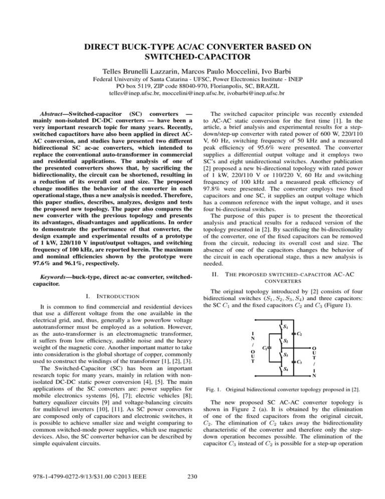
DIRECT BUCK-TYPE AC/AC CONVERTER BASED ON SWITCHED-CAPACITOR Telles Brunelli Lazzarin, Marcos Paulo Moccelini, Ivo Barbi Federal University of Santa Catarina - UFSC, Power Electronics Institute - INEP PO box 5119, ZIP code 88040-970, Florianpolis, SC, BRAZIL telles@inep.ufsc.br, moccelini@inep.ufsc.br, ivobarbi@inep.ufsc.br Abstract—Switched-capacitor (SC) converters — mainly non-isolated DC-DC converters — have been a very important research topic for many years. Recently, switched capactitors have also been applied in direct ACAC conversion, and studies have presented two different bidirectional SC ac-ac converters, which intended to replace the conventional auto-transformer in commercial and residential applications. The analysis of one of the presented converters shows that, by sacrificing the bidirectionality, the circuit can be shortened, resulting in a reduction of its overall cost and size. The proposed change modifies the behavior of the converter in each operational stage, thus a new analysis is needed. Therefore, this paper studies, describes, analyzes, designs and tests the proposed new topology. The paper also compares the new converter with the previous topology and presents its advantages, disadvantages and applications. In order to demonstrate the performance of that converter, the design example and experimental results of a prototype of 1 kW, 220/110 V input/output voltages, and switching frequency of 100 kHz, are reported herein. The maximum and nominal efficiencies shown by the prototype were 97.6% and 96.1%, respectively. Keywords—buck-type, direct ac-ac converter, switchedcapacitor. I. I NTRODUCTION It is common to find commercial and residential devices that use a different voltage from the one available in the electrical grid, and, thus, generally a low power/low voltage autotransformer must be employed as a solution. However, as the auto-transformer is an electromagnetic transformer, it suffers from low efficiency, audible noise and the heavy weight of the magnetic core. Another important matter to take into consideration is the global shortage of copper, commonly used to construct the windings of the transformer [1], [2], [3]. The Switched-Capacitor (SC) has been an important research topic for many years, mainly in relation with nonisolated DC-DC static power conversion [4], [5]. The main applications of the SC converters are: power supplies for mobile electronics systems [6], [7]; electric vehicles [8]; battery equalizer circuits [9] and voltage-balancing circuits for multilevel inverters [10], [11]. As SC power converters are composed only of capacitors and electronic switches, it is possible to achieve smaller size and weight comparing to common switched-mode power supplies, which use magnetic devices. Also, the SC converter behavior can be described by simple equivalent circuits. 978-1-4799-0272-9/13/$31.00 ©2013 IEEE 230 The switched capacitor principle was recently extended to AC-AC static conversion for the first time [1]. In the article, a brief analysis and experimental results for a stepdown/step-up converter with rated power of 600 W, 220/110 V, 60 Hz, switching frequency of 50 kHz and a measured peak efficiency of 95.6% were presented. The converter supplies a differential output voltage and it employs two SC’s and eight unidirectional switches. Another publication [2] proposed a new bi-directional topology with rated power of 1 kW, 220/110 V or 110/220 V, 60 Hz and switching frequency of 100 kHz and a measured peak efficiency of 97.8% were presented. The converter employs two fixed capacitors and one SC, it supplies an output voltage which has a common reference with the input voltage, and it uses four bi-directional switches. The purpose of this paper is to present the theoretical analysis and practical results for a reduced version of the topology presented in [2]. By sacrificing the bi-directionality of the converter, one of the fixed capacitors can be removed from the circuit, reducing its overall cost and size. The absence of one of the capacitors changes the behavior of the circuit in each operational stage, thus a new analysis is needed. II. T HE PROPOSED SWITCHED - CAPACITOR AC-AC CONVERTERS The original topology introduced by [2] consists of four bidirectional switches (S1 , S2 , S3 , S4 ) and three capacitors: the SC C1 and the fixed capacitors C2 and C3 (Figure 1). S1 I N / O U T C2 S2 C1 S3 C3 S4 O U T / I N Fig. 1. Original bidirectional converter topology proposed in [2]. The new proposed SC AC-AC converter topology is shown in Figure 2 (a). It is obtained by the elimination of one of the fixed capacitors from the original circuit, C2 . The elimination of C2 takes away the bidirectionality characteristic of the converter and therefore only the stepdown operation becomes possible. The elimination of the capacitor C3 instead of C2 is possible for a step-up operation S1 S1 S1 S1 S2 I N O U T C1 S3 C3 S4 O U T / S2 O U T S3 C1 / I N C2 vi I N / I N S4 (a) Buck-type topology (b) Boost-type topology Fig. 2. Unidirectional topologies. S2 S2 vi C1 S3 S3 C3 vo C3 vo S4 S4 (a) (b) Fig. 4. Buck converter topological states. (boost-type), as shown in Figure 2 (b). Both cases must be feeding on a source with voltage characteristics. This paper studies in detail the step-down version (buck-type) presented in Figure 2 (a). III. / O U T C1 T HEORETICAL ANALYSIS A detailed low-frequency (input voltage frequency) and high-frequency (switching frequency) theoretical analysis of the step-down converter is presented in this section. A. Topological stages The proposed converter presents two topological stages during its operation, which are controlled by the switch gate signals shown in Figure 3. The switches S1 and S3 operate together, as well as S2 and S4 . The duty-cycle of all the switches is 0.5, and S1 /S3 gate signals are complimentary of the S2 /S4 gate signals. The switching logic is very simple and can be achieved with a single UC3525 IC. B. High-frequency (HF) analysis The operational stages of the converter are discussed in this section. The closed-switch resistance non-ideality (Ron ), as well as a load resistance Ro >> Ron are taken into consideration. The analysis is detailed only for the positive half-cycle of the input voltage because the operational stages are very similar in the negative half-cycle; however, the voltages and the directions of the currents in the elements are the opposite from those of the positive half-cycle. C 1 2Ron S3 C 1 2R on S1 S3 S1 C3 vi Ro C3 vi Δt1A Ro Δt1B (a) First stage (∆t1 ) S2 S2 2R on 2Ron C3 C1 Ro C3 Ro C1 S4 S4 Δt2A Δt2B (b) Second stage (∆t2 ) Fig. 5. Buck converter operational stages in the positive half-cycle. Fig. 3. Gate signals of the bi-directional switches. In the first stage, S1 and S3 are turned on, and S2 and S4 are turned off. The converter operates with C1 and C3 seriesconnected, as shown in Figure 4 (a). In this stage, the circuit becomes a simple voltage divider and output voltage is vi/2. In the second stage, S2 and S4 are turned on, and S1 and S3 are turned off. The converter works with C1 and C3 parallel-connected, as shown in Figure 4 (b). In this stage, the input voltage source is disconnected from the circuit and the capacitor C1 works to maintain a voltage equilibrium with C3 . Therefore, the SC C1 applies and maintains a voltage in C3 equal to vi/2, i.e., the converter supplies an output voltage equal to vi/2. 231 • • First stage (∆t1 ) — starts when the switches S1 and S3 are closed. During ∆t1A , the capacitors are series-connected and receive energy from the voltage source. When the current in C3 reaches zero, it starts discharging (∆t1B ). C1 charges during the whole stage. The switches S1 and S3 are then opened and the stage is concluded. Figure 5 (a) illustrates this topological stage. The currents in S1 , S2 , S3 , S4 , C1 and C3 and the voltages vi , vo and across C1 during this stage (∆t1 ) are presented in Figure 6 (a) for the positive half-cycle and in Figure 6 (b) for the negative half-cycle. Second stage (∆t2 ) — starts when the switches S2 and S4 are closed. The capacitors are parallel-connected and the voltage source is disconnected from the circuit. C1 charges C2 during ∆t2A . When the current in C2 reaches zero, both capacitors start discharging (∆t2B ). The opening of S2 and S4 marks the end of the stage. Figure 5 (b) illustrates this topological stage. The currents and the voltages during this stage (∆t2 ) are also presented in Figure 6 (a) for positive half-cycle and Figure 6 (b) for negative half-cycle. vi Gv = vo vC3 vi = = = 0.5 vi vi 2 × vi vi_max/2 vi + input voltage. The theoretical LF waveforms of the proposed converter are shown in Figures 7 (a), 7 (b) and 7 (c). _ vi_max vi vi_max /2 vo iS3 iS3 ωt (b) Capacitor voltages ωt vS1 =vS2 =vS3 =vS4 vi_max/2 0 (a) Input and output voltages 0 0 vC1 =vC3 0 0 iS1 (1) ωt iS1 (c) Switch voltages Fig. 7. Main low frequency waveforms. iS2 0 iS4 D. Equivalent model According to [2], an equivalent circuit for the proposed converter, shown in Figure 8, can be obtained. The calculations are based on (2) — presented in [12] —, where fs is the switching frequency, Req is the equivalent resistance and D, the duty-cycle. 0 iS2 iS4 iC1 iC3 iC1 iC3 0 0 Req = 1 × fs C −1 1 − e (2fs Ron C) vo vC1 −(1−D) −D DTS Δt2B (1-D)TS (a) Δt1A (2) 0.5vi vC1 vo Δt1A Δt1B Δt2A 1 1 − e (2fs Ron C) + e (2fs Ron C) + e (2fs Ron C) 0.5vi Δt1B Δt2A DTS Req Δt2B (1-D)TS vi_eq Ceq Ro_eq vo (b) Fig. 6. High-frequency waveforms: (a) positive half-cycle, (b) negative half-cycle. Fig. 8. Equivalent circuit of the proposed converter. C. Low-frequency (LF) analysis Considering C1 and C3 equal capacitors, the voltage across each one of them tends to be vi/2 in both series and parallel stages. The maximum voltage across the switches is also vi/2. As vo is the voltage across C3 and vC3 is ideally vi/2, the voltage gain (Gv ) is calculated by (1). Thus, the converter presents the behavior of a voltage divider for any type of input voltage (AC or DC). Therefore, if a sinusoidal voltage is connected to the input of the converter, it outputs a sinusoidal voltage equal to half the 232 As shown in [2], the lowest Req is obtained with D = 0.5 and, consequently, the voltage drop and energy losses are minimized for that duty-cycle value. Eq. (3) shows the calculation of Req for a 50% duty-cycle. −1 Req(D=0.5) = 1 + e /(2fs Ron C) 1 × fs C 1 − e − 1/(2fs Ron C) (3) Table I summarizes the calculated value of the circuit elements. TABLE I Circuit elements Parameter Proposed converter Original converter [2] Ceq CeqL = 2C CeqL = 3C Req ReqL = Req ReqL = Req Vi Vi 2 2 Vi eq IV. E XPERIMENTAL R ESULTS In order to verify the proposed converter operation, a prototype was built in laboratory. The experimental results and a comparison with the original bidirectional converter is presented within this section. Table II shows the converter specifications, which are similar to the specifications of the original converter, since that allows a better comparison. The waveforms were recorded with rated power output and a 0.4 duty-cycle (0.1 dead-time). TABLE II Converter specifications Description Input Voltage Output Voltage Output Power Input Voltage Frequency Switching Frequency Capacitors MOSFET Ron Fig. 10. Input and output voltages (100 Hz). Figure 7. The voltage stresses on internal components is one half of the input voltage vi . Figure 12 shows vS1 detailed at switching frequency, which reveals the waveform does not present overvoltage. Value 220 V 110 V 1000 W 60 Hz 100 kHz 20 µF 0.06 mΩ Figures 9 and 10 show the input and output voltages. As expected, the converter works with a voltage gain of 0.5, i.e., vo is one half of vi . The frequency of the input voltage is 60 Hz in Figure 9 and, in Figure 10, is 100 Hz. This shows the converter operates normally for different input voltage frequencies. Fig. 11. Voltages across S1 , C1 and C3 (vo ). Fig. 9. Input and output voltages (60 Hz). The voltages across the switch S1 and capacitors C1 and C3 can be seen in Figure 11. Those experimental waveforms are very similar to the theoretical waveforms presented in 233 Figure 13 shows the voltage and current outputs supplied by the converter at rated power (1 kW) with a resistive load. The measured output voltage was 106.6 V, which correponds to a regulation near 96.9%. The input voltage and the input current at the rated power can be seen in Figure 14. The input current ii presents a high frequency component and it leads the voltage by approximately 10◦ , which is expected due to the topological stages of the converter and the circuit being capacitive. If the voltage source can not supply the high frequency component of the input current, a filter must be added to the converter. The frequency of the current ripple is high (100 kHz), and, thus, a small LC filter is sufficient. That configuration was also tested, with C = 10µF and L = 5µH. The current is supplied by the source, i.e., before the LC filter, can be also seen in Figure 14. The current is is approximately sinusoidal and without distortion. TABLE III Results comparison Description Peak efficiency Efficiency (1 kW) Power factor (1 kW) Voltage regulation Original [2] 97.8% 96.2% 96.9% 96.9% Proposed 97.6% 96.1% 98.5% 96.9% original bidirectional converter. A negligible loss of efficiency (due to the disconnection of the voltage source in the second operational stage), similar regulation and higher power factor are observed in the new converter results, as Table III shows. Fig. 12. Voltage across S1 detailed at 100 kHz. Fig. 15. Efficiency The experimental efficiency curve plotted in Figure 15 shows that, for a wide range of loads, the experimental efficiency is higher than 96%. The measured efficiency at rated power was 96.1% and the efficiency peak were 97.6% and occurred at approximately 400 W. Figure 15 also shows the efficiency curve of the original converter studied in [2], making evident the proposed circuit reduction does not decrease significantly the efficiency of converter. Fig. 13. Output voltage and current. Fig. 14. Input voltage (vi ), current supplied by the source (is ) and converter input current (ii ). Fig. 16. Regulation Figures 15, 16 and 17 show the efficiency, regulation and power factor, respectively, of the proposed converter and the 234 The output regulation curve can be seen in Figure 16. A voltage drop of less than 3.5% was noted for rated power compared to the no-load output voltage. Again, the proposed and original converters showed similar results. The input power factor curves plotted in Figure 17 show that the power factor is close to one at rated power, but it drops considerably as active power decreases. That is a consequence of the capacitive circuit and the parameters chosen. The comparison between the original and proposed converters demonstrates that the latter performs better in terms of input power factor, measured 98.5% at rated power. Those characteristics were expected due to fact the total capacitance of the circuit was reduced. Fig. 17. Power Factor V. C ONCLUSIONS A new switched-capacitor AC-AC converter was proposed with the following characteristics: no inductors or other magnetic elements present, only capacitors and switches employed; operation in open-loop; common reference between input and output voltages; and step-down operation with a voltage gain of 0.5. The proposed converter topology was based on another SC AC-AC converter, but with the number of capacitors reduced. Consequently, the cost and size of converter were also reduced, although, as a disadvantage, the converter became unidirectional. The paper presented the theoretical analysis of the converter and its operation was verified through experimental results. The measured maximum and rated power efficiencies were 97.6% and 96.1%, respectively. The voltage gain measured in rated power was 0.485. A comparison between the new and the original converter showed that both presented similar performance. Therefore, the proposed converter presents the advantage of a reduced number of capacitors and the disadvantage of being unidirectional. Those characteristics indicate the new converter is an appropriate alternative solution for the auto-transformer in unidirectional and low cost applications. 235 REFERENCES [1] T. B. Lazzarin, R. L. Andersen, G. B. Martins, and I. Barbi, “A 600-w switched-capacitor ac–ac converter for 220 v/110 v and 110 v/220 v applications,” IEEE Transactions on Power Electronics, vol. 27, no. 12, pp. 4821–4826, 2012. [2] R. Andersen, T. Lazzarin, and I. Barbi, “A 1 kw step-up/step-down switched-capacitor ac-ac converter,” vol. 28, pp. 3329–3340, 2013. [3] R. B. Gordon, M. Bertram, and T. Graedel, “Metal stocks and sustainability,” Proceedings of the National Academy of Sciences of the United States of America, vol. 103, no. 5, pp. 1209–1214, 2006. [4] A. Ioinovici, “Switched-capacitor power electronics circuits,” Circuits and Systems Magazine, IEEE, vol. 1, no. 3, pp. 37–42, 2001. [5] M. S. Makowski and D. Maksimovic, “Performance limits of switched-capacitor dc-dc converters,” in Power Electronics Specialists Conference, 1995. PESC’95 Record., 26th Annual IEEE, vol. 2. IEEE, 1995, pp. 1215–1221. [6] F. Z. Peng, F. Zhang, and Z. Qian, “A magnetic-less dc-dc converter for dual-voltage automotive systems,” Industry Applications, IEEE Transactions on, vol. 39, no. 2, pp. 511–518, 2003. [7] F. Zhang, L. Du, F. Z. Peng, and Z. Qian, “A new design method for high-power high-efficiency switchedcapacitor dc–dc converters,” Power Electronics, IEEE Transactions on, vol. 23, no. 2, pp. 832–840, 2008. [8] Z. Amjadi and S. S. Williamson, “A novel control technique for a switched-capacitor-converter-based hybrid electric vehicle energy storage system,” Industrial Electronics, IEEE Transactions on, vol. 57, no. 3, pp. 926–934, 2010. [9] C. Pascual and P. T. Krein, “Switched capacitor system for automatic series battery equalization,” in Applied Power Electronics Conference and Exposition, 1997. APEC’97 Conference Proceedings 1997., Twelfth Annual, vol. 2. IEEE, 1997, pp. 848–854. [10] B. Axelrod, Y. Berkovich, and A. Ioinovici, “A boostswitched capacitor-inverter with a multilevel waveform,” in Circuits and Systems, 2004. ISCAS’04. Proceedings of the 2004 International Symposium on, vol. 5. IEEE, 2004, pp. V–884. [11] Y. Hinago and H. Koizumi, “A switched-capacitor inverter using series/parallel conversion with inductive load,” Industrial Electronics, IEEE Transactions on, vol. 59, no. 2, pp. 878–887, 2012. [12] J. W. Kimball and P. T. Krein, “Analysis and design of switched capacitor converters,” in Applied Power Electronics Conference and Exposition, 2005. APEC 2005. Twentieth Annual IEEE, vol. 3. IEEE, 2005, pp. 1473–1477.


