HBL5006: LED Failure Detector and Backup LED Circuit for Critical
advertisement

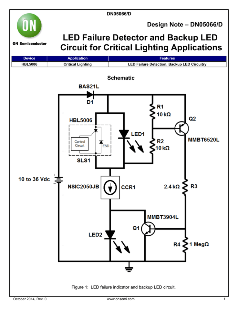
DN05066/D Design Note – DN05066/D LED Failure Detector and Backup LED Circuit for Critical Lighting Applications Device Application Features HBL5006 Critical Lighting LED Failure Detection, Backup LED Circuitry Schematic Figure 1: LED failure indicator and backup LED circuit. October 2014, Rev. 0 www.onsemi.com 1 DN05066/D Overview Although LEDs are more robust than incandescent or fluorescent lights, it is possible for LEDs to fail. These failures can be due to mechanical damage, prolonged use, manufacturing defects, and other varied causes. ON Semiconductor produces LED current bypass shunts for management of LED failures. They are multipurpose devices that allow current to flow around an LED and support detection and diagnostics of LED failures. Circuit Description The circuit shown in this design note uses an ON Semiconductor HBL5006 LED shunt to serve multiple purposes. Referencing the schematic in Figure 1, LED1 is the primary LED. This is the LED which operates from the time the lighting module is manufactured until the LED itself fails. When LED1 does fail, either as an open or a short, the circuit detects this and immediately switches in a backup LED, which is LED2. The logic of the HBL5006 device makes this near perfect continuity of the light output possible. Circuit Operation In normal operation, LED1 is operational. D1, LED1, CCR1, and Q1 are all conducting. CCR1 is a 50 mA constant current regulator. R1 and R2 form a voltage divider across LED1. When LED1 is operational, there is enough voltage at the emitter-base of Q2 to allow it to be on. When Q2 is on, the base-emitter of Q1 is also high. Q1 serves to short out LED2, preventing it from emitting light. If there is a short circuit across LED1, then D1, LED1, CCR1, and LED2 are all conducting. This is because of the R1, R2 voltage divider which controls Q2. This will prevent Q1 from being on. When Q1 is off, LED2 is no longer shorted out and can conduct current and emit light. R4 diverts Q2’s leakage current from Q1. An LED1 open circuit failure will immediately cause the HBL5006 device to turn on. When this device turns on there is an approximately 1 V drop across LED1. This makes an LED1 open circuit failure resemble a short circuit failure to Q2. This allows current to bypass the open circuit and it makes Q1 and Q2 switch. The input voltage range (approximately 10 to 36 V as shown) is determined by several factors. These are the forward voltage drop of D1, the 8.0 V maximum breakover voltage of the HBL5006, the IV characteristics of CCR1, and the voltage drop across Q2. The upper range is determined by the heat sinking available for the CCR, which is a linear current regulator. A higher input voltage is acceptable as long as the maximum power dissipation of the CCR for the given heat sinking available to it is not exceeded. Reverse protection is provided up to 250 V by D1. Forward surge is managed by the 120 V breakdown of CCR1. The circuit is easily scalable to higher currents. The ON Semiconductor CCR portfolio ranges from 10 to 350 mA, and devices can be paralleled. The LED shunt portfolio supports currents well above 1.0 A. A larger diode for D1 might be chosen such as MRA4003 and a Darlington transistor or MOSFET may be used for Q2. Bill of Materials Designator Manufacturer Part Number Qty Description Value CCR1 ON Semi NSIC2050B 1 Constant Current Regulator 120 V, 50 mA D1 ON Semi BAS21L 1 Diode 250 V, 200 mA LED1, LED2 Cree MX-6 2 LED 3 V, 1 A Q1 ON Semi MMBT6520L 1 PNP Transistor 350 V, 500 mA Q2 ON Semi MMBT3904L 1 NPN Transistor 40 V, 200 mA R1, R2 Any - 2 Resistor 10 kΩ, 1/8 W R3 Any - 1 Resistor 2.4 kΩ, 1/8 W R4 Any - 1 Resistor 1 MegΩ, 1/8 W SLS1 ON Semi HBL5006 1 LED Current Bypass Shunt 350 mA October 2014, Rev. 0 www.onsemi.com 2 DN05066/D Waveforms Figure 2: LED1 open circuit failure. LED2 turns on about 20 μs after LED1 fails. Figure 3: LED1 short circuit failure. LED2 turns on about 7 μs after LED1 fails. 1 © 2014 ON Semiconductor. Disclaimer: ON Semiconductor is providing this design note “AS IS” and does not assume any liability arising from its use; nor does ON Semiconductor convey any license to its or any third party’s intellectual property rights. This document is provided only to assist customers in evaluation of the referenced circuit implementation and the recipient assumes all liability and risk associated with its use, including, but not limited to, compliance with all regulatory standards. ON Semiconductor may change any of its products at any time, without notice. Design note created by Andrew Niles, e-mail: Andrew.Niles@ONSemi.com October 2014, Rev. 0 www.onsemi.com 3

