Read the paper
advertisement
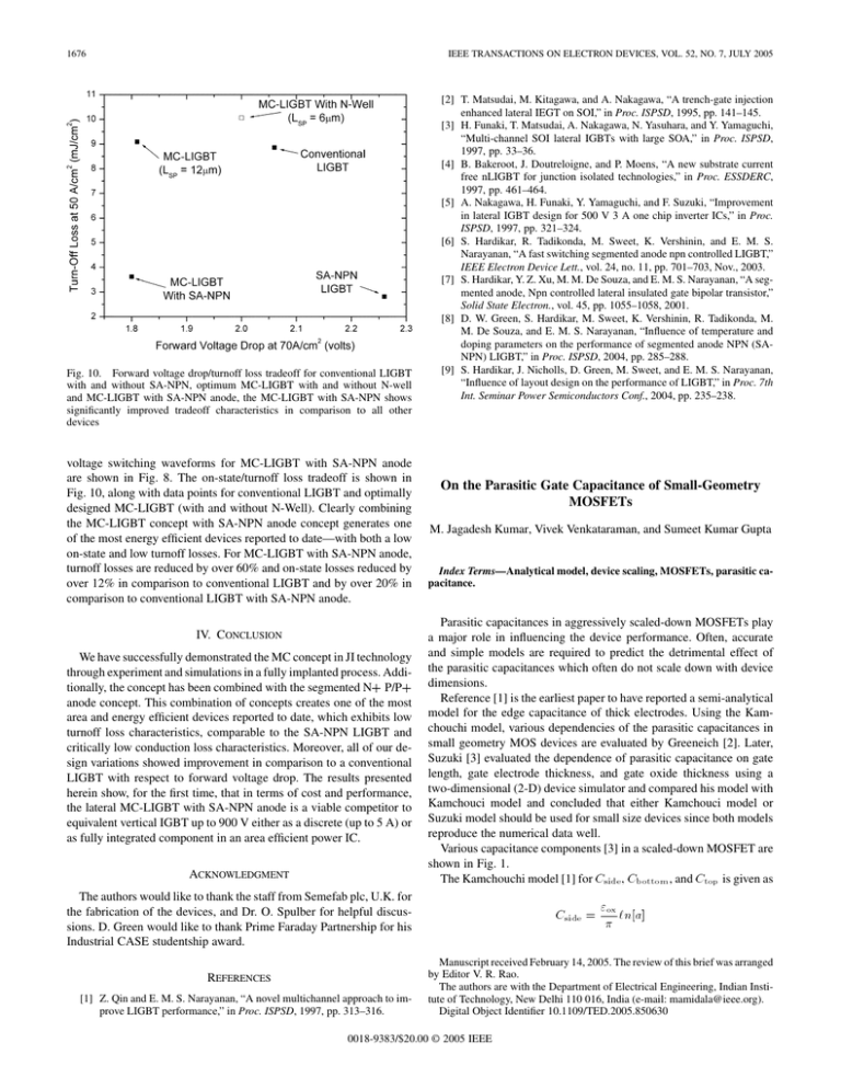
1676 IEEE TRANSACTIONS ON ELECTRON DEVICES, VOL. 52, NO. 7, JULY 2005 Fig. 10. Forward voltage drop/turnoff loss tradeoff for conventional LIGBT with and without SA-NPN, optimum MC-LIGBT with and without N-well and MC-LIGBT with SA-NPN anode, the MC-LIGBT with SA-NPN shows significantly improved tradeoff characteristics in comparison to all other devices voltage switching waveforms for MC-LIGBT with SA-NPN anode are shown in Fig. 8. The on-state/turnoff loss tradeoff is shown in Fig. 10, along with data points for conventional LIGBT and optimally designed MC-LIGBT (with and without N-Well). Clearly combining the MC-LIGBT concept with SA-NPN anode concept generates one of the most energy efficient devices reported to date—with both a low on-state and low turnoff losses. For MC-LIGBT with SA-NPN anode, turnoff losses are reduced by over 60% and on-state losses reduced by over 12% in comparison to conventional LIGBT and by over 20% in comparison to conventional LIGBT with SA-NPN anode. IV. CONCLUSION We have successfully demonstrated the MC concept in JI technology through experiment and simulations in a fully implanted process. Additionally, the concept has been combined with the segmented N+ P/P+ anode concept. This combination of concepts creates one of the most area and energy efficient devices reported to date, which exhibits low turnoff loss characteristics, comparable to the SA-NPN LIGBT and critically low conduction loss characteristics. Moreover, all of our design variations showed improvement in comparison to a conventional LIGBT with respect to forward voltage drop. The results presented herein show, for the first time, that in terms of cost and performance, the lateral MC-LIGBT with SA-NPN anode is a viable competitor to equivalent vertical IGBT up to 900 V either as a discrete (up to 5 A) or as fully integrated component in an area efficient power IC. ACKNOWLEDGMENT [2] T. Matsudai, M. Kitagawa, and A. Nakagawa, “A trench-gate injection enhanced lateral IEGT on SOI,” in Proc. ISPSD, 1995, pp. 141–145. [3] H. Funaki, T. Matsudai, A. Nakagawa, N. Yasuhara, and Y. Yamaguchi, “Multi-channel SOI lateral IGBTs with large SOA,” in Proc. ISPSD, 1997, pp. 33–36. [4] B. Bakeroot, J. Doutreloigne, and P. Moens, “A new substrate current free nLIGBT for junction isolated technologies,” in Proc. ESSDERC, 1997, pp. 461–464. [5] A. Nakagawa, H. Funaki, Y. Yamaguchi, and F. Suzuki, “Improvement in lateral IGBT design for 500 V 3 A one chip inverter ICs,” in Proc. ISPSD, 1997, pp. 321–324. [6] S. Hardikar, R. Tadikonda, M. Sweet, K. Vershinin, and E. M. S. Narayanan, “A fast switching segmented anode npn controlled LIGBT,” IEEE Electron Device Lett., vol. 24, no. 11, pp. 701–703, Nov., 2003. [7] S. Hardikar, Y. Z. Xu, M. M. De Souza, and E. M. S. Narayanan, “A segmented anode, Npn controlled lateral insulated gate bipolar transistor,” Solid State Electron., vol. 45, pp. 1055–1058, 2001. [8] D. W. Green, S. Hardikar, M. Sweet, K. Vershinin, R. Tadikonda, M. M. De Souza, and E. M. S. Narayanan, “Influence of temperature and doping parameters on the performance of segmented anode NPN (SANPN) LIGBT,” in Proc. ISPSD, 2004, pp. 285–288. [9] S. Hardikar, J. Nicholls, D. Green, M. Sweet, and E. M. S. Narayanan, “Influence of layout design on the performance of LIGBT,” in Proc. 7th Int. Seminar Power Semiconductors Conf., 2004, pp. 235–238. On the Parasitic Gate Capacitance of Small-Geometry MOSFETs M. Jagadesh Kumar, Vivek Venkataraman, and Sumeet Kumar Gupta Index Terms—Analytical model, device scaling, MOSFETs, parasitic capacitance. Parasitic capacitances in aggressively scaled-down MOSFETs play a major role in influencing the device performance. Often, accurate and simple models are required to predict the detrimental effect of the parasitic capacitances which often do not scale down with device dimensions. Reference [1] is the earliest paper to have reported a semi-analytical model for the edge capacitance of thick electrodes. Using the Kamchouchi model, various dependencies of the parasitic capacitances in small geometry MOS devices are evaluated by Greeneich [2]. Later, Suzuki [3] evaluated the dependence of parasitic capacitance on gate length, gate electrode thickness, and gate oxide thickness using a two-dimensional (2-D) device simulator and compared his model with Kamchouci model and concluded that either Kamchouci model or Suzuki model should be used for small size devices since both models reproduce the numerical data well. Various capacitance components [3] in a scaled-down MOSFET are shown in Fig. 1. The Kamchouchi model [1] for Cside ; Cbottom , and Ctop is given as The authors would like to thank the staff from Semefab plc, U.K. for the fabrication of the devices, and Dr. O. Spulber for helpful discussions. D. Green would like to thank Prime Faraday Partnership for his Industrial CASE studentship award. REFERENCES [1] Z. Qin and E. M. S. Narayanan, “A novel multichannel approach to improve LIGBT performance,” in Proc. ISPSD, 1997, pp. 313–316. Cside = "ox `n[a] Manuscript received February 14, 2005. The review of this brief was arranged by Editor V. R. Rao. The authors are with the Department of Electrical Engineering, Indian Institute of Technology, New Delhi 110 016, India (e-mail: mamidala@ieee.org). Digital Object Identifier 10.1109/TED.2005.850630 0018-9383/$20.00 © 2005 IEEE IEEE TRANSACTIONS ON ELECTRON DEVICES, VOL. 52, NO. 7, JULY 2005 1677 with R= u01 : u0a However, we have noticed that in [2] and [3], the models for Ctop and Cbottom have been interchanged as given below Fig. 1. Ctop = Schematic geometry of conductor silicon capacitance [3]. and Cbottom = where a = 2K (K 2 0 1)1=2 + 2K 0 1 t K =1+ p tox " Cbottom = ox 2 0 `n4 0 `n 1 0 2 exp and Ctop = = 1+ LG 2tox "ox u `n a where u is determined from LG 2 tox 02 a01 R pa R2 0 1 + `n "ox 2 0 `n4 0 `n 1 0 2 exp 02 1+ LG 2tox "ox u : `n a It is important to use the correct models for Ctop and Cbottom as given in [1] since each of these capacitances, if considered independently, will have a different effect on the device performance. The aim of this brief is to bring the above to the notice of the readers so that a similar error is not carried forward in future studies. REFERENCES paR + 1 a + 1 paR 0 1 0 pa `n R+1 R01 [1] H. Kamchouchi and A. Zaky, “A direct method for the edge capacitance of thick electrodes,” J. Phys. D, Appl. Phys., vol. 8, pp. 1365–1371, 1975. [2] E. W. Greeneich, “An analytical model for the gate capacitance of small geometry MOS structures,” IEEE Trans. Electron Devices, vol. ED-30, no. 12, pp. 1838–1839, Dec. 1983. [3] K. Suzuki, “Parasitic capacitance of sub-micrometer MOSFETs,” IEEE Trans. Electron Devices, vol. 46, no. 9, pp. 1895–1900, Sep. 1999.
