Latch Operation Revisited System Design with Flip-Flops Flip
advertisement

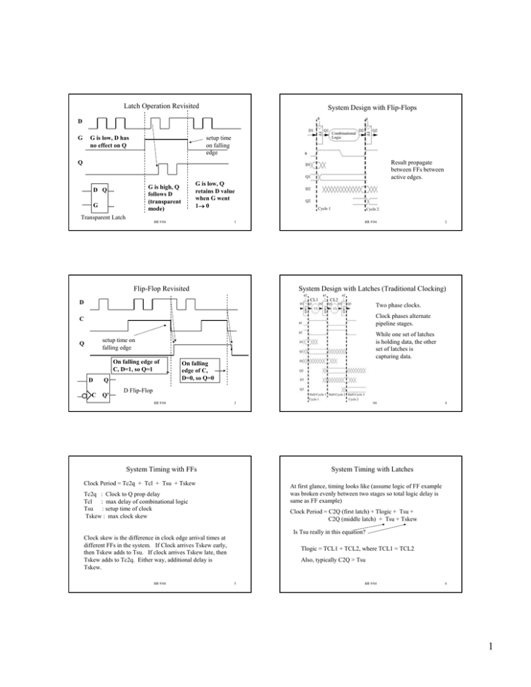
Latch Operation Revisited System Design with Flip-Flops D G is low, D has no effect on Q G setup time on falling edge Q Result propagate between FFs between active edges. G is low, Q retains D value when G went 1→ 0 G is high, Q follows D (transparent mode) D Q G Transparent Latch BR 9/04 1 Flip-Flop Revisited BR 9/04 2 System Design with Latches (Traditional Clocking) CL1 D CL2 Two phase clocks. Clock phases alternate pipeline stages. C While one set of latches is holding data, the other set of latches is capturing data. setup time on falling edge Q On falling edge of C, D=1, so Q=1 D C Q Q’ On falling edge of C, D=0, so Q=0 D Flip-Flop BR 9/04 3 System Timing with FFs 4 System Timing with Latches Clock Period = Tc2q + Tcl + Tsu + Tskew At first glance, timing looks like (assume logic of FF example was broken evenly between two stages so total logic delay is same as FF example) Tc2q : Clock to Q prop delay Tcl : max delay of combinational logic Tsu : setup time of clock Tskew : max clock skew Clock Period = C2Q (first latch) + Tlogic + Tsu + C2Q (middle latch) + Tsu + Tskew Is Tsu really in this equation? Clock skew is the difference in clock edge arrival times at different FFs in the system. If Clock arrives Tskew early, then Tskew adds to Tsu. If clock arrives Tskew late, then Tskew adds to Tc2q. Either way, additional delay is Tskew. BR 9/04 BR 9/04 Tlogic = TCL1 + TCL2, where TCL1 = TCL2 Also, typically C2Q > Tsu 5 BR 9/04 6 1 Latch Timing a L A T Tcq(b) > Tsu Tcl1 φ1 L A T CL1 φ2 CL2 Tcq(b) Tcl1 L A T φ1 Lat_a values propagate, lat_a is closed, so values are stable φ2 Latch Timing with Skew c b φ1 φ2 φ2 Tcl2 Tcq(c) Lat_b values propagate, lat_b is closed, so values are stable φ2 Tcq(b) Because Tcq > Tsu, then Tsu is satisified. Lat_c outputs stable BR 9/04 7 Any skew causes overlap which can create a race condition. System Timing with Latches (actual) Actual latch equation is: Clock Period = 2* C2Q + Tlogic + Tskew assume harmful skew BR 9/04 0 φ2 Exaggerated overlap skew 8 Skew, Clock buffer delay can cause clocks to overlap φ1 φ2 9 How much overlap can be tolerated? Shortest Path Race-thru nb Tcq(c) Phases will overlap by at least inverter delay. BR 9/04 0 Tcl2 skew Skew, Clock buffer Delay Tcq > Tsu na skew hurts in this case, setup time violation Lat_b values propagate, lat_b is closed, so values are stable Tlogic = TCL1 + TCL2, where TCL1 = TCL2 a L A T Tcq(c) skew helps in this case Lat_a values propagate, lat_a is closed, so values are stable Lat_a outputs stable Lat_b outputs stable Tcl2 Lat_a values propagate, lat_a is closed, so values are stable Lat_b values propagate, lat_b is closed, so values are stable Tcl1 φ1 Tcq(b) nc 1 BR 9/04 10 How much overlap can be tolerated? b L nd A T 0 Need to satisfy: 2*Tc2q + Tcl1 (min path) + Tcl2 (min path)+ Tsu > Toverlap Let Tcl (min path) = Tcl1(min path) + Tcl2 (min path). φ1 φ2 φ1 nc nd na nb If all of overlap due to Tskew, then: nc assumed stable ‘1’ to Lat_b 2*Tc2q + Tcl (min path) + Tsu > Tskew Race condition, wrong value in φ1 latch (lat_b). Shortest path from φ1 latch output back to φ1 latch input BR 9/04 Tcl(min path) > Tskew – 2*Tcq – Tsu 11 BR 9/04 12 2 Clock Borrowing a CL2 can borrow from CL1 b L A T CL1 φ2 L A T CL2 φ1 Tcl1+Tcq_b Lat_a values propagate, lat_a is closed, so values are stable Not always possible to perfectly balance logic delays in each stage. φ2 Tsu φ1 φ2 Clock Borrowing can be useful c L A T Tcl2+Tcq_c Latches allow us to do clock borrowing. Tsu Helps alleviate the pipeline balancing problem. Lat_b values propagate, lat_b is closed, so values are stable Note that CL2 can borrow from CL1, but not vice-versa. BR 9/04 13 BR 9/04 Can we do clock borrowing in Flip-Flop System? 14 If DFF has positive Setup time, No Clock Borrowing a To do clock borrowing in a FF-system, we need a FF with negative setup time (input can change after active clock edge) b D F F CL1 c D F F CL2 D F F Master/Slave DFF Design D D Q D Q C G G φ1 Q φ1 φ1 φ1 Tc2q_a + TCL1 + Tsu + Tskew Tc2q_b + TCL2 + Tsu + Tskew Rising edge-triggered, Tsu of FF is whatever Tsu is for the master latch (assume it is positive) BR 9/04 15 Rising Edge DFF using Pulsed Latch design D D Q C Cp BR 9/04 16 Clock Borrowing in DFF system (DFFs with negative Tsu) c a b D D D F F F CL1 CL2 F F F Q G Pulse Gen φ1 φ1 negative Tsu φ1 φ1 Tsu of internal latch (positive) C Tc2q_a + TCL1 + Cp Tsu of FF (negative!) BR 9/04 17 Want negative Tsu to be > Tskew to eliminate Skew. Tskew Tc2q_b + TCL2 + BR 9/04 Tskew 18 3 Pulsed Latch Design (AMD-K6) Timing Summary • Ck Latch-based System – – – • M1 Allows clock borrowing System timing is: Clock period = Tcl (phase1) + Tcl (phase2) + 2*Tc2q +Tskew If clock phase overlap, then: Tcl(min path of Tcl1, Tcl2) > Tskew – 2*Tcq – Tsu – Ck_dly_b Pulse gen M1 Y M2 M5 Ck_dly_b M1 off M2 on D affects Y M4 on, M6 off Ck_dly_b = 1 M1 Ck_dly_b = 0 21 M7 M5 Ck_dly_b Vdd Ck 1 → 0 M1 on M2 off, M8 off Ck_dly_b = 0 D F F φ1 Vdd Y = Vdd Q = Qold M4 off M6 on M10 off BR 9/04 22 Static Cmos D F F φ1 Static Cmos D F F φ1 Clock period = Tcq + Tcl (max) Y = Vdd M4 off M6 on M10 off BR 9/04 Vdd Qb M10 M4 M10 M4 Pipelined DFF System (pulsed Latches) with Static CMOS Q M9 M6 Qb M9 M1 off M2 on Ck 1 M8 M3 M5 Vdd M10 on Y M7 M6 Q new = Not (Y) M2 Y Q M8 M3 Ck_dly_b Pulsed Latch Design (AMD-K6) D M1 D BR 9/04 Ck 20 M2 Vdd Vdd Ck 0 → 1 Ck Qb M10 M4 M10 on, M6 off Pulsed Latch Design (AMD-K6) M9 M6 Q = Qold BR 9/04 M8 M3 D M7 off M8 off M4 on Q M7 M10 Vdd Vdd M1 on, Y=Vdd M2 off Ck_dly_b = 1 Ck M9 M4 19 Pulsed Latch Design (AMD-K6) M5 M6 Ck =0 Qb M8 M3 D DFFs with positive Setup: Clock Period = Tc2q + Tcl (max) + Tsu + Tskew DFFs with negative Setup: Clock period = Tcq + Tcl (max) if Tsu (negative) > Tskew BR 9/04 M7 M2 DFF-based System – Y Q Q = Qold 23 if Tsu (negative) > Tskew Desireable Feature: want DFFs with low latency (small Tcq) BR 9/04 24 4 Pipelined Latch System with Static CMOS a L A T b Static Cmos φ1 Level-Sensitive Latch Design c L A T L A T Static Cmos φ2 φ1 Clock Period = 2* Tc2q + Tcl (max path) If clock phase overlap, then: Tcl(min path) > Tskew – Tcq – Tsu (to avoid racethru) BR 9/04 25 TSPC = True Single Phase Clocking (clock does not have to inverted), use on Alpha 21064 (first Alpha, one LARGE clock driver). TSPC latches slower than traditional latches, easy to invert clock locally. BR 9/04 26 Flip-Flop Design • Can combine TSPC Latches in several ways to make a Flip-Flop Node X is a dynamic node. If clock =1 and D=0, then node is floating! Lowers noise immunity, susceptible to charge sharing, charge coupling. Note that this FF has a long latency. BR 9/04 Cgd BR 9/04 Y BR 9/04 28 Cgd Cgs between wires due to sidewall capacitance or layer-to-layer capacitance When channel is off, Cgs = Cgd = 0 When channel is saturated (on), Cgs, Cgd is maximized. Wire C Cgs M1 Gate and Source/Drain Coupling Charge coupling is where a signal transition on one node causes a voltage change on another node via a coupling capacitor. Charge coupling Wire B X 27 What is Charge Coupling? Wire A Charge coupling problem on this node. Node is truly dynamic, will be a case where it is not driven. M2 Charge coupling between gate and source/drain due to Cgs, Cgd. 29 Gate and Source/Drain coupling is a problem when the coupled node is not being actively driven (which is the case for a dynamic node). BR 9/04 30 5 Clk X Charge Coupling Problem in Negative Edge TPSC Dff M2 Clk M1 Clk Note that X is precharged low, which turns on M1, maximizing charge coupling to node X from Y. Y Clk Clk Only effect in this case is a slowing down of rise time of node Y, this will adversely affect H to L transition on output (TPHL) Y pulled high by M1, M2 Y X For Vdd=3.3, 0.25u: Node X has charge coupled to it from Y going high, turns off M1 somewhat, slows Y transition. X precharged low BR 9/04 Node X, note charge coupling. TPHL = 273 ps, TPLH = 90 31 BR 9/04 New Simulation How to fix this? X M1 Clk Clk M2 Y Clk 32 Swap positions of M1, M2. Note that both source and drain of M1 are now precharged high, eliminating charge coupling problem. Clk Node X Note that charge coupling is eliminated. For Vdd=3.3, 0.25u: BR 9/04 33 A Pulsed DFF TPHL = 195 ps (improved by 30%) TPLH = 85 ps BR 9/04 Operation CK Dynamic node, not actively driven during most of evaluation From: F. Klass, et.al., “A New Family of Semidynamic and Dynamic Flip-Flops with Embedded Logic for High-Performance Processors, IJSSC, Vol 34, No 5, May 1999. BR 9/04 34 35 High impedance when CK=0 Hold time = Ton time; Ton length is critical – too short, metastability, too long then hold time impacts performance. BR 9/04 36 6 Improved Design Why NAND Gate? Keeper ensures output always actively driven. Keeper gets rid of dynamic node. Pulldown path conditional with value of D. If D=1, then X=0, making S=1 Suitable for interfaces to static logic. Note that output is stable through precharge. BR 9/04 37 Spice Simulation Results In Precharge, CK=0, CKD=0, X=1, S=H, N1 = ON. At Eval start, CK=1 (N3 on), CK=0, X=1. If D=1, then N2 on, so X pulled low. X going low forces S to stay high, resulting in more robust pulldown of node X. This is called “conditional shutoff” – N1 is not shutoff if D=1. BR 9/04 38 Embedded Logic With conditional shutoff. Delay from CK to CKD decreased from 100ps to 10 ps in 10 ps steps (decreasing TON sampling window) Original circuit without conditional shutoff. Note failure of pulldown of node X. Conditional shutoff allows smaller TON times. BR 9/04 39 Dynamic DFF BR 9/04 40 Dynamic Dual Rail DFF Weak keeper that keeps outputs at logic ‘1’. Do not need full keeper since outputs precharged to a ‘0’. Used for interfacing to dynamic logic – output forced to a ‘0’ during precharge. BR 9/04 Embedded logic reduces number of logic stages between registers, but adds latency to DFF. Tradeoff is generally in favor of embedding logic in the DFF. Useful when true and complement outputs are required for interfacing to dynamic logic because dynamic logic cannot implement inverting logic, so dual rail inputs are required. 41 BR 9/04 42 7 Self-Resetting CMOS (SRCMOS) Pulsed DFF with self-resetting outputs • SRCMOS differs from Domino logic in that the reset signal is generated locally – Less clock load • Outputs are pulsed 0→1 → 0, inputs assumed pulsed as well Ck D Ck_dly_b M3 Causes outputs to return low for selfresetting outputs. Notice that Clock does not go to precharge pull up, only eval transistor. M4 BR 9/04 43 – Because inputs are ‘0’ at start of evaluation, then no need for evaluation transistor! – No evaluation transistor means one less transistor in pulldown path means a faster circuit • Many schemes for generating reset – Delayed version of the clock – Generate reset based on dual rail outputs – Generate reset for an entire block of gates at one time • Will look at this in more detail for decode circuits for RAMs. BR 9/04 44 8


