Quantum resistance metrology in graphene
advertisement
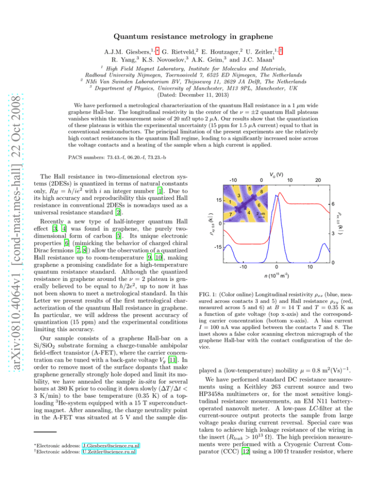
Quantum resistance metrology in graphene A.J.M. Giesbers,1, ∗ G. Rietveld,2 E. Houtzager,2 U. Zeitler,1, † R. Yang,3 K.S. Novoselov,3 A.K. Geim,3 and J.C. Maan1 We have performed a metrological characterization of the quantum Hall resistance in a 1 µm wide graphene Hall-bar. The longitudinal resistivity in the center of the ν = ±2 quantum Hall plateaus vanishes within the measurement noise of 20 mΩ upto 2 µA. Our results show that the quantization of these plateaus is within the experimental uncertainty (15 ppm for 1.5 µA current) equal to that in conventional semiconductors. The principal limitation of the present experiments are the relatively high contact resistances in the quantum Hall regime, leading to a significantly increased noise across the voltage contacts and a heating of the sample when a high current is applied. PACS numbers: 73.43.-f, 06.20.-f, 73.23.-b ∗ Electronic † Electronic address: J.Giesbers@science.ru.nl address: U.Zeitler@science.ru.nl -10 3 15 VG (V) 0 5 ρxy; 5,6 (kΩ) The Hall resistance in two-dimensional electron systems (2DESs) is quantized in terms of natural constants only, RH = h/ie2 with i an integer number [1]. Due to its high accuracy and reproducibility this quantized Hall resistance in conventional 2DESs is nowadays used as a universal resistance standard [2]. Recently a new type of half-integer quantum Hall effect [3, 4] was found in graphene, the purely twodimensional form of carbon [5]. Its unique electronic properties [6] (mimicking the behavior of charged chiral Dirac fermions [7, 8]) allow the observation of a quantized Hall resistance up to room-temperature [9, 10], making graphene a promising candidate for a high-temperature quantum resistance standard. Although the quantized resistance in graphene around the ν = 2 plateau is generally believed to be equal to h/2e2 , up to now it has not been shown to meet a metrological standard. In this Letter we present results of the first metrological characterization of the quantum Hall resistance in graphene. In particular, we will address the present accuracy of quantization (15 ppm) and the experimental conditions limiting this accuracy. Our sample consists of a graphene Hall-bar on a Si/SiO2 substrate forming a charge-tunable ambipolar field-effect transistor (A-FET), where the carrier concentration can be tuned with a back-gate voltage Vg [11]. In order to remove most of the surface dopants that make graphene generally strongly hole doped and limit its mobility, we have annealed the sample in-situ for several hours at 380 K prior to cooling it down slowly (∆T /∆t < 3 K/min) to the base temperature (0.35 K) of a toploading 3 He-system equipped with a 15 T superconducting magnet. After annealing, the charge neutrality point in the A-FET was situated at 5 V and the sample dis- 1 10 20 8 6 6 4 7 2 µm 0 3 ρxx; 3,5 ((kΩ) arXiv:0810.4064v1 [cond-mat.mes-hall] 22 Oct 2008 2 1 High Field Magnet Laboratory, Institute for Molecules and Materials, Radboud University Nijmegen, Toernooiveld 7, 6525 ED Nijmegen, The Netherlands NMi Van Swinden Laboratorium BV, Thijsseweg 11, 2629 JA Delft, The Netherlands 3 Department of Physics, University of Manchester, M13 9PL, Manchester, UK (Dated: December 11, 2013) -15 -10 0 15 10 0 -2 n (10 m ) FIG. 1: (Color online) Longitudinal resistivity ρxx (blue, measured across contacts 3 and 5) and Hall resistance ρxy (red, measured across 5 and 6) at B = 14 T and T = 0.35 K as a function of gate voltage (top x-axis) and the corresponding carrier concentration (bottom x-axis). A bias current I = 100 nA was applied between the contacts 7 and 8. The inset shows a false color scanning electron micrograph of the graphene Hall-bar with the contact configuration of the device. played a (low-temperature) mobility µ = 0.8 m2 (Vs)−1 . We have performed standard DC resistance measurements using a Keithley 263 current source and two HP3458a multimeters or, for the most sensitive longitudinal resistance measurements, an EM N11 batteryoperated nanovolt meter. A low-pass LC-filter at the current-source output protects the sample from large voltage peaks during current reversal. Special care was taken to achieve high leakage resistance of the wiring in the insert (Rleak > 1013 Ω). The high precision measurements were performed with a Cryogenic Current Comparator (CCC) [12] using a 100 Ω transfer resistor, where 2 0.4 0.4 0.4 (b) -9 -6 15 -2 n (10 m ) -3 3 6 9 15 -2 n (10 m ) 12 0.0 0.4 ρ3,5 0.2 0.2 0.0 0.0 30 -0.2 ρxx (Ω) -12 ρ4,6 (b) -0.4 0 Isd (µA) 1 ρxx (Ω) 0.0 0.2 ρ4,6 (a) ρ3,5 ρxx (Ω) 0.2 ρxx (kΩ) ρxx (kΩ) (a) -0.2 15 -0.4 0 0 FIG. 2: (Color online) (a) Detailed sweep of ρxx for holes on both sides of the sample, ρ3, 5 (red) and ρ4, 6 (blue), with Isd = 0.5 µA at B = 14 T and T = 0.35 K. The curves were taken for two different cooldowns (solid and dotted lines). (b) Detailed sweep of ρxx; 4, 6 for electrons at different sourcedrain currents, Isd = 0.5, 1.5, 2.5 µA, respectively solid black, dashed red and dotted blue at B = 14 T and T = 0.35 K. special attention was devoted to measuring at low currents (Isd = 1.5 µA). Figure 1 shows a typical quantum Hall measurement at B = 14 T and T = 0.35 K with the Hall resistance ρxy and the longitudinal resistivity ρxx plotted as a function of the carrier concentration n. Around filling factors ν = ±2 the device displays well defined flat plateaus in ρxy accompanied by zero longitudinal resistivity minima in ρxx . In a next step we characterize the sample following the metrological guidelines [13] for DC-measurements of the quantum Hall resistance, especially making sure that the longitudinal resistivity ρxx is well enough zero in order to provide a perfect quantization of ρxy [2]. Qualitatively, the absolute error in the quantization of ρxy due to a finite ρxx , can be estimated as ∆ρxy = −sρxx , where s is in the order of unity [14]. In order to address the quantization conditions in some detail, we have investigated the longitudinal resistivities in the ν = ±2 minima along both sides of the sample under different conditions. Figure 2(a) shows that the ν = −2 resistivity minima for holes are indeed robustly developed on both sides of the sample for two different cooldowns. A similar robustness of the resistivity minima is also observed for electrons around the ν = 2 minimum. Figure 2(b) displays the behaviour of ρxx around ν = 2 for increasing source-drain currents. All minima remain robust and symmetric, the position of the middle of the minimum does not change for neither the holes nor the electrons when the bias current is increased. A more detailed investigation of the longitudinal resistance in its zero-minima is shown in Figure 3. On the hole side of the sample (Fig. 3(a)) the resistivity in the ν = −2 minimum remains zero for bias currents up to 2.5 µA within the measurement noise (20 mΩ for the highest current). At higher currents the resistance starts to rise significantly above zero, indicating current breakdown of the quantum Hall effect. For electrons (Fig. 3(b)), even higher currents are attainable; no breakdown is observed for currents as high 1 2 Isd (µA) 3 0 1 2 Isd (µA) 3 FIG. 3: (Color online) Precise measurement of the zero longitudinal resistance for (a) holes (n = −7.68·1015 m−2 ), and (b) electrons (n = +7.89·1015 m−2 ) at B = 14 T and T = 0.35 K. Current densities of 2.5 A/m for holes and 3.5 A/m for electrons are achievable in graphene before the quantum Hall effect starts to breakdown (gray arrow). The inset shows the same hole measurements for a poorly annealed sample. as 3.5 µA, corresponding to a current density of 3.5 A/m. For a 1 µm wide Hall bar, this is a very promising result indeed, as wider samples might therefore easily sustain currents up to several tens of microamperes before breakdown of the quantum Hall effect starts [15]. As a reference we also investigated a poorly annealed sample (charge neutrality point at 9 V, mobility µ = 0.5 m2 (Vs)−1 at 0.35 K). Here the quantum-Hall minimum breaks down for considerably smaller currents (see insert in (Fig. 3(a)) and already reaches 30 Ω at a current of 1 µA, making it unsuitable for high precision measurements of the QHE. These characterization measurements presented so far are a promising starting point to anticipate that the Hall resistance in graphene is indeed quantized accurately. From the fact that ρxx remains below 20 mΩ for currents up to 2.5 µA one may expect an accuracy as good as 1 ppm for the quantum Hall plateaus in this well annealed sample. In order to check this expectation we performed high precision measurements on the quantum Hall plateaus using a CCC with a source-drain current of 1.5 µA (see Fig. 4). Variations measured in the quantum Hall resistance in a many hour CCC measurement (Fig. 4) were more than one order of magnitude larger than the 1 to 2 parts in 106 noise attained in a single five minute CCC measurement run. The fluctuations in the precision measurement are considerably reduced when better voltage contacts are chosen. Still, the variations were two orders of magnitude larger than in a measurement at the same current of an AlGaAs heterostructure. Combining several measurement runs using different contacts, we achieved an average resistance value of the ν = ±2 quantum Hall plateaus in graphene of RH = (12, 906.34 ± 0.20) Ω, showing no indication of a different quantization in graphene with respect to conventional two-dimensional electron systems at the level of 3 resistance, ρxx = 2.3 Ω. ∆ρxy /ρxy (ppm) 80 Rp.a. R7,8_3,4 40 Raverage 0 R7,6_8,4 -40 R7,8_5,6 -80 FIG. 4: (Color online) Deviations from quantization in ppm measured with the CCC (Isd = 1.5 µA) for different contact configurations and the average of them (blue circles). The red square (Rp.a. ) represents the deviation for a poorly annealed sample at a source-drain current of 0.5 µA. TABLE I: Contact resistances of the graphene sample, measured in the quantum Hall regime where ρxx ≃ 0 Ω (all values for the voltage contacts (1-6) were measured at 0.1 µA, whereas the current contacts 7 and 8 where measured at 3 µA). Contact # Rholes (kΩ) Relectrons (kΩ) 1 5.6 1.25 3 0.95 6.3 4 0.03 2.7 5 1.4 4.8 6 0.3 1.1 7 1.0 5.5 8 0.3 0.8 (−5 ± 15) parts in 106 . For comparison we also determined the quantization of the poorly annealed sample at a source-drain current of 0.5 µA. The deviation of (85 ± 20) ppm is consistent with an s-factor of −0.41 due to the finite longitudinal [1] K. v. Klitzing, C. Dorda, M. Pepper, Phys. Rev. Lett. 45, 494 (1980). [2] B. Jeckelmann and B. Jeanneret, Rep. Prog. Phys. 64, 1601 (2001). [3] K.S. Novoselov et al., Nature 438, 197 (2005). [4] Y. Zhang, Y. Tan, H.L. Stormer, P. Kim, Nature 438, 201 (2005). [5] A.K. Geim and K.S. Novoselov, Nature Mat. 6, 183 (2007). [6] A.H. Castro Neto, F. Guinea, N.M.R. Peres, K.S. Novoselov and A.K. Geim, Rev. Mod. Phys., in press; preprint at http://xxx.lanl.gov/abs/0709.1163 (2007). [7] G.W. Semenoff, Phys. Rev. Lett. 53, 2449 (1984). [8] F.D.M. Haldane, Phys. Rev. Lett. 61, 2015 (1988). [9] K.S. Novoselov et al., Science 315, 1379 (2007). [10] A.J.M. Giesbers et al., Phys. Rev. Lett. 99, 206903 The main limitation in the CCC measurements appeared to be the contact resistance of the voltage contacts [13]. The rather high resistances induce additional measurement noise and fluctuations in the voltage contacts thereby limiting the attainable accuracy of quantum-Hall precision experiments. Table I shows the contact resistances for our specific sample in the center of the ρxx minima around ν = ±2 in a three terminal setup. They reveal large variations for the different contacts, and, furthermore a significant difference between holes (n < 0) and electrons (n > 0). The latter might be explained by doping effects of the contacts [16] and the high contact resistance of the contacts could be accounted for by non-ideal coupling between the gold contacts and the graphene sheet. [17]. Besides noise on the voltage contacs, high contact resistances also lead to local heating at the current contacts thereby limiting the maximum breakdown current. In conclusion, we have presented the first metrological characterization of the quantum Hall effect in graphene. We have shown that the quantum Hall resistance in a only 1 µm wide graphene sample is already within (−5 ± 15) ppm equal to that in conventional AlGaAs and Si-MOSFET samples. A proper annealing of the sample ensuring well pronounced zeroes in ρxx and sufficiently high breakdown currents were shown to be crucial to obtain such an accuracy. The main limitation for high accuracy measurements in our experiments are the relatively high contact resistances of the sample used, inducing measurement noise and local heating. Extrapolating our results to samples with lower resistance contacts for both electrons and holes and using wider samples with high breakdown currents, would most probably allow precision measurements of the quantum Hall effect in graphene with an accuracy in the ppb range. (2007). [11] K.S. Novoselov et al., Science 306, 666 (2004). [12] P. Kleinschmidt, J.M. Williams, N.E. Fletcher and T.J.B.M. Janssen, IEE Proc.-Sci. Meas. Technol. 149, 302 (2002). [13] F. Delahaye and B. Jeckelmann, Metrologia 40, 217 (2003). [14] M. Furlan, Phys. Rev. B 57, 14818 (1998). [15] Graphene samples can intrinsically sustain even higher currents up to several milliamperes, see J. Moser et al., Appl. Phys. Lett. 91, 163513 (2007). [16] G. Giovannetti et al., Phys. Rev. Lett. 101, 026803 (2008). [17] E.J.H. Lee et al., Nature Nano. 3, 486 (2008).
