Discussion 4
advertisement

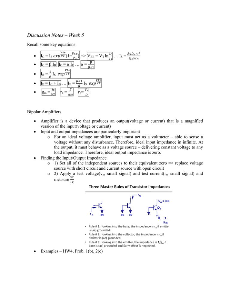
Discussion Notes – Week 5 Recall some key equations • IC = IS • IC = β IB IC = α IE … α = • IB = • IE = IC + IB … I E = • gm = (1+ => VBE = VT ln … IS = IS rπ = IS ro= Bipolar Amplifiers • • • • Amplifier is a device that produces an output(voltage or current) that is a magnified version of the input(voltage or current) Input and output impedances are particularly important o For an ideal voltage amplifier, input must act as a voltmeter – able to sense a voltage without any disturbance. Therefore, ideal input impedance in infinite. At the output, it must behave as a voltage source – delivering constant voltage to any load impedance. Therefore, ideal output impedance is zero. Finding the Input/Output Impedance o 1) Set all of the independent sources to their equivalent zero => replace voltage source with short circuit and current source with open circuit o 2) Apply a test voltage(vx, small signal) and test current(ix, small signal) and measure Examples – HW4, Prob. 1(b), 2(c) Biasing • • • • • Proper biasing is required to ensure operation in the forward active region => small signal parameters depend on the bias conditions o 1) Perform DC analysis to find the operating point(VEB and VCE => under what condition is it forward active region?) and small signal parameters o 2) Set all sources to their zero equivalent and perform small signal analysis Note: When iteration is required, it is relatively safe to assume VBE=0.7V to begin with Resistive Divider Biasing o Example 5.9 Razavi (use of Thevenin) R VCC => with assumption that the base current is negligible(relatively o Vx = R R accurate since input impedance is typically extremely high) o IC = IS = IS => even though resistance does not vary much, exponential dependence on resistance still makes it undesirable o Multiple iteration often required Biasing with Emitter Degeneration o Example 5.10 Razavi (just the set-up) o Presence of RE helps to absorb the error in VBE(variation in VBE results in a linear potential drop across RE) Self-biasing o Collector voltage provides the necessary Vx and IB. o Higher potential VC guarantees forward active region Bipolar Amplifier Topologies – Common Emitter • Voltage gain – Av = -gmRC – is negative • The voltage gain of CE stage is limited by the supply voltage VCC • • Input/output impedance is found using identical method as above Common Emitter Degeneration o Resistor connected to the emitter of CE stage • o Overall gain is reduced, but improvement in linearity and input impedance(Rin=rπ => Rin= rπ + (β+1)RE Multiple Stage CE o o We can reduce Q2 to its equivalent impedance using the method described above o Example – HW4, Prob. 4 (a), (b)


