Ripple-Precharge TCAM: A Low-Power Solution for Network Search
advertisement
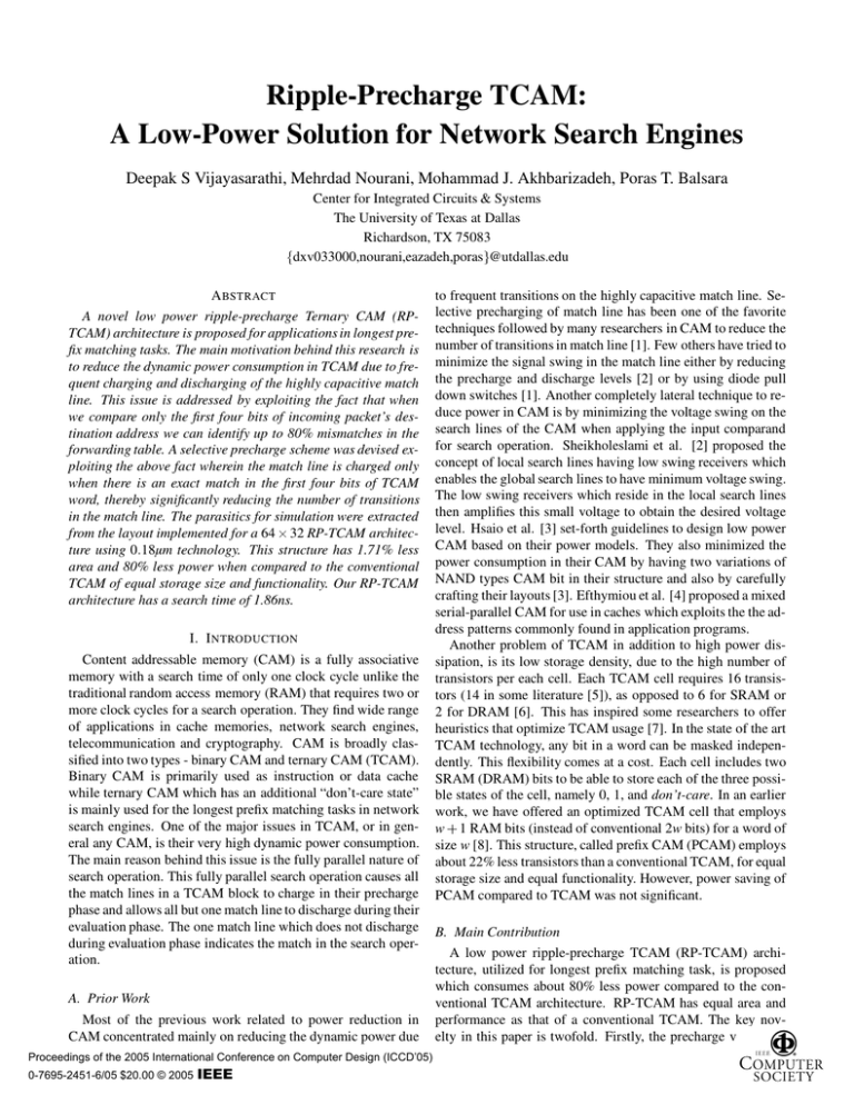
Ripple-Precharge TCAM: A Low-Power Solution for Network Search Engines Deepak S Vijayasarathi, Mehrdad Nourani, Mohammad J. Akhbarizadeh, Poras T. Balsara Center for Integrated Circuits & Systems The University of Texas at Dallas Richardson, TX 75083 dxv033000,nourani,eazadeh,poras@utdallas.edu A BSTRACT A novel low power ripple-precharge Ternary CAM (RPTCAM) architecture is proposed for applications in longest prefix matching tasks. The main motivation behind this research is to reduce the dynamic power consumption in TCAM due to frequent charging and discharging of the highly capacitive match line. This issue is addressed by exploiting the fact that when we compare only the first four bits of incoming packet’s destination address we can identify up to 80% mismatches in the forwarding table. A selective precharge scheme was devised exploiting the above fact wherein the match line is charged only when there is an exact match in the first four bits of TCAM word, thereby significantly reducing the number of transitions in the match line. The parasitics for simulation were extracted from the layout implemented for a 64 32 RP-TCAM architecture using 0 18µm technology. This structure has 1.71% less area and 80% less power when compared to the conventional TCAM of equal storage size and functionality. Our RP-TCAM architecture has a search time of 1.86ns. I. I NTRODUCTION Content addressable memory (CAM) is a fully associative memory with a search time of only one clock cycle unlike the traditional random access memory (RAM) that requires two or more clock cycles for a search operation. They find wide range of applications in cache memories, network search engines, telecommunication and cryptography. CAM is broadly classified into two types - binary CAM and ternary CAM (TCAM). Binary CAM is primarily used as instruction or data cache while ternary CAM which has an additional “don’t-care state” is mainly used for the longest prefix matching tasks in network search engines. One of the major issues in TCAM, or in general any CAM, is their very high dynamic power consumption. The main reason behind this issue is the fully parallel nature of search operation. This fully parallel search operation causes all the match lines in a TCAM block to charge in their precharge phase and allows all but one match line to discharge during their evaluation phase. The one match line which does not discharge during evaluation phase indicates the match in the search operation. A. Prior Work Most of the previous work related to power reduction in CAM concentrated mainly on reducing the dynamic power due Proceedings of the 2005 International Conference on Computer Design (ICCD’05) 0-7695-2451-6/05 $20.00 © 2005 IEEE to frequent transitions on the highly capacitive match line. Selective precharging of match line has been one of the favorite techniques followed by many researchers in CAM to reduce the number of transitions in match line [1]. Few others have tried to minimize the signal swing in the match line either by reducing the precharge and discharge levels [2] or by using diode pull down switches [1]. Another completely lateral technique to reduce power in CAM is by minimizing the voltage swing on the search lines of the CAM when applying the input comparand for search operation. Sheikholeslami et al. [2] proposed the concept of local search lines having low swing receivers which enables the global search lines to have minimum voltage swing. The low swing receivers which reside in the local search lines then amplifies this small voltage to obtain the desired voltage level. Hsaio et al. [3] set-forth guidelines to design low power CAM based on their power models. They also minimized the power consumption in their CAM by having two variations of NAND types CAM bit in their structure and also by carefully crafting their layouts [3]. Efthymiou et al. [4] proposed a mixed serial-parallel CAM for use in caches which exploits the the address patterns commonly found in application programs. Another problem of TCAM in addition to high power dissipation, is its low storage density, due to the high number of transistors per each cell. Each TCAM cell requires 16 transistors (14 in some literature [5]), as opposed to 6 for SRAM or 2 for DRAM [6]. This has inspired some researchers to offer heuristics that optimize TCAM usage [7]. In the state of the art TCAM technology, any bit in a word can be masked independently. This flexibility comes at a cost. Each cell includes two SRAM (DRAM) bits to be able to store each of the three possible states of the cell, namely 0, 1, and don’t-care. In an earlier work, we have offered an optimized TCAM cell that employs w 1 RAM bits (instead of conventional 2w bits) for a word of size w [8]. This structure, called prefix CAM (PCAM) employs about 22% less transistors than a conventional TCAM, for equal storage size and equal functionality. However, power saving of PCAM compared to TCAM was not significant. B. Main Contribution A low power ripple-precharge TCAM (RP-TCAM) architecture, utilized for longest prefix matching task, is proposed which consumes about 80% less power compared to the conventional TCAM architecture. RP-TCAM has equal area and performance as that of a conventional TCAM. The key novelty in this paper is twofold. Firstly, the precharge voltage to Data Data I/O Interface BL BL w-2 0 ... b b ... b WL 1 b b ... b w-2 WL n-1 ... w-2 ... ... w-1 b w-2 bw-1 ... ML 0 0 ML 1 0 ... w-1 b ML n-1 Priority Encoder WL 0 ... BL w-1 Address Decoder evaluate the parallel search operation is selectively and serially rippled through the first four most significant serial CAM bits. This idea exploits the fact that by just comparing the first four most significant bits of the TCAM word we can identify up to 80% of search mismatches. The second novelty in our proposed RP-TCAM architecture is that it does not have any timing signals. By eliminating the timing signals, we not only reduce the dynamic power, dissipated due to charging and discharging of such highly capacitive node, but also save energy consumed by their drivers. RAM Best Match Output (e.g. next hop) 0 ... C. Paper Organization The rest of this paper is organized as follows. Section II describes the background of packet forwarding using TCAM and different low power techniques in TCAM. The description of RP-TCAM, a customized CAM-TCAM architecture, is explained in Section III. The implementation details and the experimental results are presented in Section IV. Finally, concluding remarks are in Section V. CMPw-1 CMPw-2 Comparand (e.g. packet’s destination address) Figure 1. Packet forwarding using TCAM. TABLE I C OMPARISON IN TCAM CELL D 0 0 1 1 II. B ACKGROUND A. Packet Forwarding Using TCAM In a network router, packet forwarding is carried out by determining the next hop destination address from the forwarding table maintained in the router. A longest prefix match is done on the entries of the forwarding table for the destination address of the incoming packet. An entirely hardware based solution for carrying out longest prefix match task is using a TCAM. A typical implementation of a n w TCAM based architecture is shown in Figure 1. The forwarding table entries in TCAM consists of destination addresses along with their corresponding mask value. The destination address of an incoming packet to the router is compared with all the destination addresses stored in the TCAM to determine whether we have a match or not. The priority encoder which follows the TCAM finds the best match, i.e. the longest prefix matching in network applications. The entries are sorted such that the longest prefix destination address has the highest priority and is stored in the lower addresses of TCAM and vice versa. There are many software based solutions in existence to address the fast lookup of destination address like Patricia tree or binary search algorithm [9] but still the hardware based solution of having TCAM for IP forwarding is more advantageous solely because of their very high search speed and simplicity. The main disadvantage of the hardware based lookup using TCAM is its very high power consumption due to simultaneous switching activity of almost all cells. As an example of this fact, the average power consumption of today’s TCAM chips is in the range of 10 to 20 Watts [10]. Minimizing the power consumption is the main focus of this research. B. TCAM Architecture Figure 2 shows the basic structure of the conventional TCAM bit. The TCAM model we have assumed consists of three main components - a 8T CAM cell which stores the data bit and also compares its content (D) with the key (CMP), a 6T SRAM cell Proceedings of the 2005 International Conference on Computer Design (ICCD’05) 0-7695-2451-6/05 $20.00 © 2005 IEEE CMP 0 Address CMP 0 1 0 1 X 0 1 1 0 which stores the mask bit (MD) and a 2T XOR gate that compares the result of the CAM operation (X) with complement of mask bit (MDB) to determine whether we have a match or not. The contents of both the SRAMs are read and written using the bit lines (BL) and (BLB). (WL) and (MWL) lines are made active high for any Read/Write operation involving data or mask bit. The behavior of the TCAM cell is summarized in Table I and II. The comparand or key for the search operation is fed to the CAM cell using the comparand lines (CMP and CMPB). The match line (ML) which is connected to one end of the 2-input XOR gate is precharged to Vdd before any search operation while other end is connected to ground. The 2-input XOR gate is controlled by the output of the CAM cell (X) and the mask bit (MDB). Depending on the output of CAM cell and the mask bit, the ML either discharges when there is a mismatch or retains the charge on match. Typically during a mismatch, the mask bit MD 0 shows that the bit is a “care” bit and the CAM cell output X 1 shows that there is a mismatch between data and key. See the second row in Table II. TABLE II B EHAVIOR OF THE EVALUATION LOGIC IN TCAM. MD 0 0 1 1 X 0 1 0 1 ML Vdd 0 Vdd Vdd Meaning “care” bit; match “care” bit; mismatch “don’t-care” bit; match “don’t-care” bit; match CAM-BIT CAM-BIT WL WL DB BLB D BL DB BLB BL D CMPB CMPB CMP CMP X X EVALUATION LOGIC ML_IN ML_OUT EVALUATION LOGIC MDB Figure 3. Ripple-precharge CAM cell. ML TABLE III B EHAVIOR OF THE EVALUATION LOGIC IN RP-TCAM. MD MDB MWL MASK-BIT Figure 2. A conventional TCAM cell. C. Low-Power Techniques in TCAM There are variety of techniques by which we can reduce the power consumed in a TCAM. Inherently the structure of the TCAM bit itself has two SRAM cells which are major contributors of static power. Many circuit techniques are already in place to reduce the static power in SRAMs [11]. The other major source of power dissipation in TCAM, which is the primary concern in this work, is the dynamic power dissipation. The source of dynamic power dissipation in TCAM can be classified under one of these three categories : 1) Power consumed due to frequent charging and discharging of the highly capacitive match line. 2) Power dissipated due to charging and discharging of the search lines when the comparand or the key is applied. 3) Power dissipated due to any frequently transitioning clock node. These three categories are in coherence with the criteria putforth by researchers for any low power CAM design [3]. These criteria were put-forth based on the power models. Selective precharging has been one of the most predominant techniques used to reduce the frequent charging and discharging of match line node capacitance. A different approach to reduce power is by reducing the voltage swing across the match line. The power dissipated due to charging search line is also another major contributor to dynamic power in TCAM. Traditionally, the search lines of the CAM are combined with their corresponding bit lines. This increases the capacitance in the search line due to addition of the one extra drain capacitance by each SRAM cell on the bit line. This problem can be resolved by having separate search and bit lines. Even after separating the search line from the bit line, we see that search line through which we send the key for comparison is by itself highly capacitive. Charging Proceedings of the 2005 International Conference on Computer Design (ICCD’05) 0-7695-2451-6/05 $20.00 © 2005 IEEE D 0 0 1 1 CMP 0 1 0 1 X 0 1 1 0 ML OUT Vdd 0 Vdd 0 and discharging search line alone during every search operation dissipates a lot of power. This problem is rightly addressed by Sheikholeslami et al. wherein they propose a hierarchical search line scheme to reduce the voltage swing of the highly capacitive search line [2]. The hierarchical search line scheme consists of a low swing receiver followed by a local search line for every TCAM bit along with the global search line. Only a very small voltage is applied to the global search line which is then amplified by the low swing receiver and fed into the local search line. Several architectures proposed earlier for selective precharging used one or more transistor usually for discharging the accumulated charge in the nodes connecting any two serial transistors or the node connecting the serial transistor with the match line [1]. However, these transistors are controlled by a frequently varying signal such as clock to switch them “ON” every cycle to discharge the accumulated charge. Unfortunately, the capacitance of this clock node further increases when the clock node spans through the entire TCAM block and frequent charging and discharging of this node increases the dynamic power consumption. Moreover, the drivers, used to drive these clock nodes, also consume power. Our proposed architecture addresses these issues by eliminating any frequently varying signals thereby reducing the dynamic power consumption. III. R IPPLE -P RECHARGE TCAM A RCHITECTURE A. Concept of Ripple-Precharge The structure of the ripple-precharge CAM cell is shown in Figure 3. The main difference between the conventional TCAM cell shown in Figure 2 and this cell is in the evaluation logic. The series NMOS transistors of the evaluation circuit in Conventional TCAM Cells Ripple-Precharge CAM Cells CAM-BIT 31 Vdd CAM-BIT 30 X31 X30 CAM-BIT 29 CAM-BIT 27 CAM-BIT 28 X29 X28 CAM-BIT 26 X27 ... CAM-BIT 0 ... X26 X0 ML ... MDB26 MDB27 MDB0 LA MASK-BIT 27 MASK-BIT 26 ... MASK-BIT 0 Figure 4. 32-bit word of the proposed RP-TCAM architecture. TCAM is replaced with a PMOS transistors in the new CAM. The source of the PMOS transistor is connected to ML IN and its drain is connected to the drain of the discharging NMOS transistor whose source is grounded. The node which connects PMOS and the NMOS transistor is connected to the ML OUT line which is in turn connected to the ML IN line of the next bit. Therefore, the PMOS transistors in series ripple Vdd only when there is an exact match in the most significant four bits of the RP-TCAM word. The additional NMOS transistor connected to the ML OUT node of the parallel PMOS transistors ripples a 0 whenever there is a mismatch. The match line in the parallel part of the RP-TCAM is thus selectively charged by the rippling Vdd only when there is a match in the first 4 most significant bits. The behavior of the evaluation logic for a ripple-precharge CAM cells is summarized in Table III. B. Circuit Behavior The novel RP-TCAM architecture consists of both rippleprecharge CAM bits and conventional TCAM bits as shown in Figure 4. The first four most significant bits of the RP-TCAM word are intentionally CAM bits and not TCAM bits. This architectural change can be validated from the fact that most significant eight bits of the packet are never masked [12]. Further, the elimination of mask bit from the first four most significant bits of the TCAM is justified from the results of packet profiling [13]. This is mainly due to hierarchical structure of internet protocol (IP) address allocation in classless inter-domain routing (CIDR). Therefore, the first four most significant bits of the proposed 32-bit RP-TCAM word are CAM bits and the least significant twenty eight bits are TCAM bits. RP-TCAM architecture initially evaluates the first four most significant bits of the search key serially. If there is an exact match between the current data bit stored in the SRAM and the corresponding comparand bit sent through CMP and CMPB lines, the Vdd ripples through the current bit to evaluate the next bit. If there is a mismatch in any of the first four bits of the ripple-precharge CAM a 0 is propagated to the next bit from current mismatched bit. The match line in the second part is charged to Vdd only when there is a match in the first four CAM bits. Whenever there is a mismatch in any one of the three most significant bits of the RP-TCAM, a 0 is propagated to the next Proceedings of the 2005 International Conference on Computer Design (ICCD’05) 0-7695-2451-6/05 $20.00 © 2005 IEEE bit as shown in Table III. If this 0 starts to ripple through the subsequent bits i.e. considering subsequent bits to have an exact match, we might end up having a Vt (threshold voltage) drop at match line (ML). In order to avoid this and have a clear distinction between a match and mismatch, an inverter followed by a discharge transistor is connected to ML as shown in Figure 4. The input of the inverter (LA) is connected to the ML OUT of the 29th bit of the RP-TCAM word. This is done in order to forsee a Vt rippling through the series PMOS transistor and avoid having Vt drop in match line for a mismatch. The number of CAM bits through which the Vdd is to be rippled is quite small for all practical packet traces and routing tables that we have tried so far. In what follows, show one such simulation. The simulation results are obtained using the forwarding table taken from the AS1221 edge router on June 10, 2004 and has 168,178 active IPv4 route prefixes [14] and the packet trace from the main router of a national laboratory used also in [15]. The objective behind this simulation is to find out the percentage of prefix mismatch corresponding to N most significant bits of the incoming packet. The simulation results shown in Figure 5 reflect the percentage of searches in which mismatch discovered in the first N most significant bits (100α%). N 4 is a very good choice because by just 4 most significant bits of the packets destination address we can determine 80% of the prefix mismatches. We did not choose N 3 because the percentage of prefix mismatch was only 60% for 3 bits when compared to 80% for N 4. On the other hand, choosing N 4 is not advisable because we will have performance penalty as the search time will increase. C. Power Analysis 1 Dynamic power consumption is given by Pdyn 2 Cload 2 , where, C f Vdd is the load capacitance switched, Vdd is load the supply voltage and f is the frequency of transitions on that particular node. In our application, for n word memory modules we have: PTCAM n PML n 1 2 2 CML f TCAM Vdd (1) PRP TCAM n PML n 1 2 CML f RP TCAM 2 Vdd NAME LP/PS DB RR MD ML(RP) 110.0 ML(RP) 0 0 0 ML(CONV) 4 0 0 100.0 90.0 Mismatch for N bits (%) 80.0 70.0 60.0 50.0 ML(CONV) 40.0 30.0 20.0 0.0 1.0 2.0 3.0 4.0 5.0 6.0 7.0 8.0 9.0 10.0 Number of bits (N) 11.0 12.0 13.0 14.0 15.0 16.0 17.0 Figure 5. Percentage of mismatch (100α%) when N most significant bits are used. 0.3 Suppose α is the fraction of searches that lead to a mismatch and found through checking the first 4 bits. Based on what we discussed so far, in RP-TCAM architecture we expect this fraction to be large which means that on average 100α% of searches 4 experience 32 f TCAM transitions and the rest see all-bit transitions in a word. In other words: TCAM α 4 32 1 α f TCAM 32 32 ∆P TCAM 30.3 50.3 NANO SECONDS 40.3 90.3 80.3 70.3 60.3 100.3 Average Power 0.0 7 1 α f TCAM 8 −0.05 The total saving that RP-TCAM architecture that will achieve will be: PTCAM PRP PTCAM 20.3 Figure 6. Signal waveform on the match line for RP-TCAM (top curve) and TCAM (bottom curve). f TCAM f RP f TCAM TCAM 7 α (2) 8 −0.1 −0.15 Power (Watts) f RP 10.3 (95.179n, −0.0038481) (95.152n, −0.015902) −0.2 −0.25 −0.3 −0.35 As explained in the previous section, in most practical cases of network search engines, 0 8 α 0 9 (see Figure 5). This is equivalent to power saving (∆P%) of 70.0% to 78.8%. −0.4 Power (Watts) : Time (s) TCAM −0.45 RP−TCAM −0.5 0.0 IV. I MPLEMENTATION AND R ESULTS A. Layout Implementation The layouts of the proposed 32-bit RP-TCAM architecture as well as the conventional TCAM architecture were drawn using Cadence tools using 0 18µm Digital CMOS process [16]. The supply voltage was fixed at Vdd 1 8V . The parasitics were extracted for both the layouts and the circuit simulation was done using SPICE3 [17]. The resulting waveform of the match line for 32-bit RP-TCAM and TCAM word are shown in Figure 6. In the RP-TCAM architecture the match line (top curve) charges to Vdd only when there is an exact match between the TCAM word entry and the input comparand, unlike the conventional TCAM architecture wherein the match line (bottom curve) precharges during every search operation and discharges during all but one search operation. The waveforms comparing the time average power consumed by both architectures are shown in Figure 7. This is done by applying 50 keys (longest prefix searchers) and using transistor-level (SPICE) simulator [17]. Proceedings of the 2005 International Conference on Computer Design (ICCD’05) 0-7695-2451-6/05 $20.00 © 2005 IEEE 10n 20n 30n 40n 50n Time (s) 60n 70n 80n 90n 100n Figure 7. Average power consumed by TCAM and RP-TCAM architectures. The layouts for 64 32 bit RP-TCAM block and conventional TCAM block were drawn and are shown in 8. It’s obvious that there is no area increase in RP-TCAM. Table IV shows the comparison of time average power, area and search time of the conventional TCAM and proposed RP-TCAM architectures. A negative number in the last column shows improvement in area and power. We can clearly see that, even for 50 searches, the average power consumed by the RP-TCAM architecture is found to be almost 75.79% less than the conventional architecture. RP-TCAM has an area saving of 1.71% with 2.76% degradation in performance. B. Comments on Design and Implementation Issues The most significant four bits of the CAM are arranged in a manner that they occupy the area equivalent to two TCAM Figure 8. Layouts of 64 32 RP-TCAM and TCAM architectures. TABLE IV C OMPARISON OF 64 32 CONVENTIONAL AND PROPOSED TCAM ARCHITECTURE . Comparison Metric Area (mm2 ) Search Time (ns) Average Power (mW ) TCAM 0.292 1.81 15.90 RP-TCAM 0.287 1.86 3.85 Change [%] -1.71 +2.76 -75.79 cells. Therefore, we have an area saving of two TCAM bits when compared to the conventional TCAM architecture. The additional overhead of an inverter and NMOS transistor to discharge the match line is very negligible when compared to the other very recent architectures [4] which has much higher area overhead. The ripple-precharge CAM bit has PMOS transistors in its evaluation logic when compared to conventional TCAM which has NMOS transistors. This makes the size of evaluation logic for that part CAM a little bigger than that of its TCAM counterpart. Overall, we have an area saving of 1.71% compared to the conventional TCAM architecture. In Figure 6 we see that there is a small glitch in the match line of the proposed RP-TCAM architecture. The glitch is due to the corner case wherein the mismatch occurs in the least significant 28 bits and not in the most significant 4 bits of the TCAM. The effect of this mismatch is that both charging and evaluation of match line of RP-TCAM takes place at the same time. This effect is minimized by making the PMOS transistors of the serial TCAM weaker i.e by decreasing their sizes at the same time not compromising on performance. Another important design constraint which we face is the leakage current during a mismatch in the first four most significant bit. During mismatch, the output of the CAM cell (X) is Vdd -Vtn and not Vdd . This makes the PMOS transistor to leak. This issue can be addressed either by having a transmission gate logic in evaluation transistors or by having high Vt transistors. Proceedings of the 2005 International Conference on Computer Design (ICCD’05) 0-7695-2451-6/05 $20.00 © 2005 IEEE V. C ONCLUSION This paper presents a novel, low power TCAM architecture used for longest prefix matching tasks in network search engine applications. Our proposed RP-TCAM architecture implements the idea of rippling Vdd to selectively precharge the highly capacitive match line. The condition for precharging the match line is derived from the fact that more than 80% of mismatch can be identified by just comparing the first four bits of the prefixes. By exploiting this inherent property of the prefixes we designed our RP-TCAM. Both the conventional TCAM and proposed RP-TCAM were implemented in 0 18µm technology. The average power consumed by the proposed RP-TCAM is found to be 75 79% less than that of the conventional TCAM. The area of the RP-TCAM is found to be 1 71% less than that of conventional TCAM for equal storage size and functionality. Our RP-TCAM architecture has a search time of 1 86ns. ACKNOWLEDGEMENTS This work has been supported in part by the Cisco Systems Academic Research and Technology Initiative Award. R EFERENCES [1] C.A. Zukowski and S.Y. Wang, “Use of selective precharge for low-power content-addressable memories,” In Proceedings of the IEEE International Symposium on Circuits and Systems, Vol. 3, pages 1788-1791, 1997. [2] K. Pagiamtzis and A. Sheikholeslami, “Pipelined match-lines and hierarchical search-lines for low-power content-addressable memories,” In Proceedings of the IEEE Custom Integrated Circuits Conference, pages 383-386, 2003. [3] I.Y.L. Hsiao, D.H. Wang, and C.W. Jen, “Power modeling and low-power design of content addressable memories,” In Proceedings of the IEEE International Symposium on Circuits and Systems,Vol. 4, pages 926-929, 2001. [4] Aristides Efthymiou and Jim D.Garside, “A CAM with Mixed Serial-Parallel comparison for use in Low Energy Caches,” IEEE Transactions on Very Large Scale Integration Systems,Vol. 12, no. 3, Mar. 2004. [5] I. Arsovski, T. Chandler, and A. Sheikholeslami, “A Ternary Content-Addressable Memory (TCAM) Based on 4T Static Storage and Including a Current-Race Sensing Scheme,” IEEE Journal of Solid-State Circuits, vol. 38, no. 1, January 2003. [6] J. Rabaey, Digital Integrated Circuits, Prentice Hall, 1996. [7] H. Liu, “Routing Table Compaction in Ternary CAM,” IEEE Micro, January, February 2002. [8] M. Akhbarizadeh, M. Nourani, D. Vijayasarathi, P. Balsara, “PCAM: A Ternary CAM Optimized for Packet Forwarding Tasks,” IEEE International Conference on Computer Design, October 2004. [9] Pei, T.-B., Zukowski, C. “Putting Routing Tables in Silicon,” IEEE Network Magazine, January 1992, 42-49. [10] Integrated Device Technology, Inc., www.idt.com, 2005. [11] Chris h. Kim and Kaushik Roy, “Dynamic Vt SRAM : A Leakage Tolerant Cache Memory for Low Voltage Microprocessors,” In Proceedings of ISLPED’02, August 2002. [12] RFC1519, the Internet Engineering Task Force, www.ietf.org, 2005. [13] Internet Performance Measurement and Analysis Project, Univ. of Michigan and Merit Network Inc., www.merit.edu, 2005. [14] bgp.potaroo.net, “BGP Routing Table Analysis Reports,” 2004. [15] T. Chiueh and P. Pradham, “Cache Memory Design for Internet Processors,” IEEE Micro, February 2000. [16] Cadence Design Systems Inc., “Virtuoso Layout Editor Users Guide - Version 4.4.6,” June 2000. [17] Texas Instruments Inc., “TI Spice3 User’s and Reference Manual - Version 1.6,” 1994.
