MPQ2489-AEC1
Step-Down White LED Driver
with Wide 6V–55V Input Voltage
AEC-Q100 Qualified
DESCRIPTION
FEATURES
The MPQ2489 is a high efficiency step-down
converter designed in continuous current mode
for driving the high brightness Light Emitting
Diodes (LED) from wide input voltage 6V–55V.
•
•
•
•
•
•
•
•
•
•
•
•
The MPQ2489 employs hysteretic control
architecture to regulate a high accuracy LED
current, which is measured through an external
high-side current sensing resistor. Moreover,
this control scheme provides optimized circuit
stabilization and very quick response time
without the loop compensation. Its low 202mV
average feedback voltage reduces power loss
and improves the converter efficiency.
The MPQ2489 implements PWM and analog
dimming together with DIM pin.
The MPQ2489 includes thermal overload
protection preventing damage in the event of an
output overload.
The MPQ2489 is available in small QFN6 (3x
3mm) and SOIC8E packages.
•
Guaranteed Industrial/Automotive Temp
Internal 60V MOSFET
Wide 6V to 55V Input Range
≥1A Output Current
High Efficiency (>95%)
Hysteresis Control
PWM & Analog Dimming
1000:1 PWM Dimming Resolution
Thermal Shutdown
Inherent Open LED Protection
Short LED Protection
Available in QFN6(3x 3mm) and SOIC8E
Packages
Available in AEC-Q100 Grade 1
APPLICATIONS
•
•
•
•
•
Low Voltage Halogen Replacement
Low Voltage General Illumination
Automotive/Decorative LED Lighting
Signs/Emergency Lighting
LED Backlighting
All MPS parts are lead-free and adhere to the RoHS directive. For MPS green
status, please visit MPS website under Products, Quality Assurance page.
“MPS” and “The Future of Analog IC Technology” are registered trademarks of
Monolithic Power Systems, Inc.
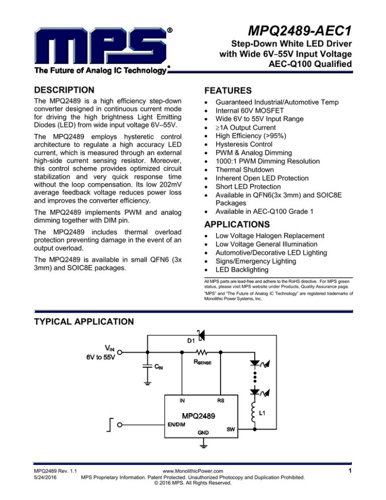
TYPICAL APPLICATION
MPQ2489 Rev. 1.1
www.MonolithicPower.com
5/24/2016
MPS Proprietary Information. Patent Protected. Unauthorized Photocopy and Duplication Prohibited.
© 2016 MPS. All Rights Reserved.
1
MPQ2489 – STEP DOWN WLED DRIVER WITH WIDE 6V~55V INPUT VOLTAGE, AEC-Q100 QUALIFIED
ORDERING INFORMATION
Part Number
MPQ2489DQ*
MPQ2489DQ-AEC1**
MPQ2489DN-AEC1***
Package
QFN-6 (3x3mm)
QFN-6 (3x3mm)
SOIC8E
Top Marking
9Y
9Y
MP2489
* For Tape & Reel, add suffix -Z (e.g. MPQ2489DQ-Z).
For RoHS Compliant Packaging, add suffix -LF (e.g. MPQ2489DQ-LF-Z)
** For Tape & Reel, add suffix -Z (e.g. MPQ2489DQ-AEC1-Z).
For RoHS Compliant Packaging, add suffix -LF (e.g. MPQ2489DQ-AEC1-LF-Z
*** For Tape & Reel, add suffix -Z (e.g. MPQ2489DN-AEC1-Z).
For RoHS Compliant Packaging, add suffix -LF (e.g. MPQ2489DN-AEC1-LF-Z
PACKAGE REFERENCE
QFN-6 (3x 3mm)
SOIC8E
ABSOLUTE MAXIMUM RATINGS (1)
VIN, VSW ........................................ -0.3V to +60V
VRS ................................................. VIN-5V to VIN
All Other Pins .............................. -0.3V to +6.3V
Continuous Power Dissipation
(TA = +25°C) (2)
QFN6 .........................................................2.5W
SOIC8E .....................................................2.5W
Junction Temperature .............................. 150°C
Lead Temperature ................................... 260°C
Storage Temperature ............... -65°C to +150°C
Recommended Operating Conditions
(3)
Supply Voltage VIN ............................. 6V to 55V
Operating Junction Temp. (TJ). -40°C to +125°C
Thermal Resistance
(4)
θJA
θJC
QFN-6 (3mm x 3mm) ............. 50 ...... 14 ... °C/W
SOIC8E .................................. 50 ...... 10 ... °C/W
Notes:
1) Exceeding these ratings may damage the device.
2) The maximum allowable power dissipation is a function of the
maximum junction temperature TJ(MAX), the junction-toambient thermal resistance θJA, and the ambient temperature
TA. The maximum allowable continuous power dissipation at
any ambient temperature is calculated by PD(MAX)=(TJ(MAX)TA)/ θJA. Exceeding the maximum allowable power dissipation
will cause excessive die temperature, and the regulator will go
into thermal shutdown. Internal thermal shutdown circuitry
protects the device from permanent damage.
3) The device is not guaranteed to function outside of its
operation conditions.
4) Measured on JESD51-7, 4-layer PCB.
MPQ2489 Rev. 1.1
www.MonolithicPower.com
5/24/2016
MPS Proprietary Information. Patent Protected. Unauthorized Photocopy and Duplication Prohibited.
© 2016 MPS. All Rights Reserved.
2
MPQ2489 – STEP DOWN WLED DRIVER WITH WIDE 6V~55V INPUT VOLTAGE, AEC-Q100 QUALIFIED
ELECTRICAL CHARACTERISTICS
VIN = 24V, TJ = -40°C to +125°C unless otherwise noted. Typical values are at TJ = 25°C.
Parameter
Symbol Condition
Input Voltage
VIN
Shutdown Supply Current
ISD
Min
6
TJ =25°C
Quiescent Supply Current
Internal Reference Voltage
Feedback Reference Voltage
(with respect to VIN)
Feedback Reference Voltage
Hysterisis
EN/DIM Max Dimming Voltage
EN/DIM Mim Dimming Voltage
EN/DIM Enable High Voltage
EN/DIM Enable Low Volatge
EN/DIM Up-pulling Resistor
Recommended PWM Dimming
(5)
Frequency
IQ
VREF
VIN = 24V
85
55
V
108
1.23
1.275
1
1.32
192
202
212
217
±30
VDIM MAX
VDIM MIN
VEN HIGH VEN Rising
VEN LOW VEN Falling
REN
FPWM
mV
2.56
0.3
V
V
V
V
kΩ
2
kHz
0.3
0.16
45
0.1
Ω
ns
ns
0.5
100
100
30
External capacitor on dim pin
is 4.7nF
mA
V
mV
187
VFB_HYS
TSS
Units
130
No Switching
TJ =25°C
VIN-VRS VEN/DIM = 1.28V T = -40°C to
J
+125°C
Max
µA
TJ = -40°C to
+125°C
Switch On Resistance
RDS ON
(6)
Minimum On Time
TON MIN
(6)
Minimum Off Time
TOFF MIN
Recommended
Maximum
FMAX
Operating Frequency
Recommended Duty Cycle
D
(5)
Range at FMAX
Start Up Time
Typ
0.3
600
kHz
70
%
0.5
ms
Notes:
5) Application recommendation, no production test.
6) Design Guarantee, no production test.
MPQ2489 Rev. 1.1
www.MonolithicPower.com
5/24/2016
MPS Proprietary Information. Patent Protected. Unauthorized Photocopy and Duplication Prohibited.
© 2016 MPS. All Rights Reserved.
3
MPQ2489 – STEP DOWN WLED DRIVER WITH WIDE 6V~55V INPUT VOLTAGE, AEC-Q100 QUALIFIED
PIN FUNCTIONS
QFN6
Pin#
SOIC8E
Pin#
1
1
2, 5
2, 3, 6, 7
3
4
4
5
6
8
Name Description
The Drain of Internal MOSFET. Connecting the common terminal of inductor and
anode of Schottky to this pin.
GND Ground.
Enable/Dimming Command Input. To use PWM dimming, apply a square wave
signal to this pin. To use Analog dimming, apply a 0.3V–2.5V DC voltage to this
EN/DIM pin. The voltage from 0.3V to 2.5V linearly controls the LED current range from
25% to 200%. Turn off the output current when pulling this pin below 0.2V.
Connect a 1nF–10nF capacitor for normal operation (VEN/DIM=1.28V).
LED Current Sense Input. Connecting the current sensing resistor that programs
RS
the LED average current to IN pin.
IN
Input Supply Pin. Connecting a proper decoupling capacitor from IN pin to GND.
SW
MPQ2489 Rev. 1.1
www.MonolithicPower.com
5/24/2016
MPS Proprietary Information. Patent Protected. Unauthorized Photocopy and Duplication Prohibited.
© 2016 MPS. All Rights Reserved.
4
MPQ2489 – STEP DOWN WLED DRIVER WITH WIDE 6V~55V INPUT VOLTAGE, AEC-Q100 QUALIFIED
TYPICAL PERFORMANCE CHARACTERISTICS
VIN=30V, 3 LEDS in series, IOUT=550mA, unless otherwise noted.
MPQ2489 Rev. 1.1
www.MonolithicPower.com
5/24/2016
MPS Proprietary Information. Patent Protected. Unauthorized Photocopy and Duplication Prohibited.
© 2016 MPS. All Rights Reserved.
5
MPQ2489 – STEP DOWN WLED DRIVER WITH WIDE 6V~55V INPUT VOLTAGE, AEC-Q100 QUALIFIED
TYPICAL PERFORMANCE CHARACTERISTICS (CONTINUED)
VIN=30V, 3 LEDS in series, IOUT=550mA, unless otherwise noted.
MPQ2489 Rev. 1.1
www.MonolithicPower.com
5/24/2016
MPS Proprietary Information. Patent Protected. Unauthorized Photocopy and Duplication Prohibited.
© 2016 MPS. All Rights Reserved.
6
MPQ2489 – STEP DOWN WLED DRIVER WITH WIDE 6V~55V INPUT VOLTAGE, AEC-Q100 QUALIFIED
FUNCTION DIAGRAM
Figure 1—MPQ2489 Function Block Diagram
MPQ2489 Rev. 1.1
www.MonolithicPower.com
5/24/2016
MPS Proprietary Information. Patent Protected. Unauthorized Photocopy and Duplication Prohibited.
© 2016 MPS. All Rights Reserved.
7
MPQ2489 – STEP DOWN WLED DRIVER WITH WIDE 6V~55V INPUT VOLTAGE, AEC-Q100 QUALIFIED
OPERATION
Steady State
System Soft Start
The MPQ2489 is a hysteretic controlled step
down LED driver that is easily to be configured in
varies applications ranging from 6V–55V input.
The converter employs a high side current
sensing resistor to detect and regulate the LED
current. The voltage across the current sensing
resistor is kept measured and regulated in
202mV±30mV range.
The voltage on the EN/DIM pin is the inductor
current reference. An external capacitor from the
EN/DIM pin to ground provides a soft-start delay.
When VIN starts, internal voltage source charges
the capacitor from 0V to 1.25V to fulfill soft-start
function.
The internal 1.275V reference voltage is utilized
to provide a 0.2V reference for enabling the part
and a 1.275V pulling-up voltage as current
reference voltage. When VEN>0.2V, the output
of the comparator becomes high and the other
blocks are enabled.
Output current is sensed by high-side resistor
Rsense. When the switch is on, R2 is shorted
and output current upper-threshold is fixed by R1.
When the switch is off, output current lowerthreshold is fixed by R1 and R2. Ratio of R1 and
R2 determines the current hysteresis.
Enable Control
Once Input voltage is applied, the internal 1.275V
reference is connected to EN/DIM pin through
pull up resistor. If EN/DIM is left open, the IC will
automatically start up to the maxim brightness.
Appling a capacitor on this pin can hereby
program a soft start time.
Dimming Control
MPQ2489 provides two dimming methods: PWM
dimming and DC analog dimming.
To use PWM dimming, apply a square wave to
the EN/DIM pin. To use analog dimming, apply a
0.3V–2.5V DC voltage to this pin.
Maximum Continuous Switching Current
MPQ2489 max continuous switching current
depends on the package with different thermal
resistance. The table 1 shows the max
continuous current corresponding package for
reference.
Table 1. IMAX vs. Package
Package
QFN6
Imax(A)
1.41
If an external voltage range from 1.275V to 1.25V
is applied to this pin, the current sensing voltage
reference is linearly controlled from 0mV to
202mV. By controlling the EN/DIM pin voltage
the analog dimming can be easily employed.
If an external PWM voltage is applied on this pin,
the IC will follow the PWM duty to achieve the
PWM dimming, the PWM signal amplitude must
be about 1.25V. About the flexible external PWM
dimming method, please refer to the selecting
dimming control mode section.
MPQ2489 Rev. 1.1
www.MonolithicPower.com
5/24/2016
MPS Proprietary Information. Patent Protected. Unauthorized Photocopy and Duplication Prohibited.
© 2016 MPS. All Rights Reserved.
8
MPQ2489 – STEP DOWN WLED DRIVER WITH WIDE 6V~55V INPUT VOLTAGE, AEC-Q100 QUALIFIED
APPLICATION INFORMATION
Setting the LED Current
The LED current is identical and set by the
current setting resistor between the IN pin and
RS pin.
inductor current reference directly and linearly
controls the inductor current range from 25% to
200%. (See Figure 2)
RSET=202mV/ILED
For RSET=0.36Ω, the LED current is set to 550mA
Selecting the Diode
The output diode supplies current to the inductor
when the internal MOSFET is off. To reduce
losses due to diode forward voltage and recovery
time, use a Schottky diode with the MPQ2489.
The diode should be rated for a reverse voltage
greater than the input voltage. The average
current rating must be greater than the maximum
load current expected, and the peak current
rating must be greater than the peak inductor
current.
Selecting the Input Capacitor
The input capacitor reduces the surge current
drawn from the input supply and the switching
noise from the device. A 10µF–22µF capacitor is
enough for most application. The voltage rating
should be greater than input voltage. A low ESR
capacitor should be used for input decoupling.
Selecting the Output Capacitor
For most applications, output capacitor is not
necessary. But if peak to peak ripple LED current
is required less than 30% of average current, add
a capacitor across the LEDs. Proportionally lower
ripple can be achieved with higher capacitor
value. A value of 2.2µF will meet most
requirements.
Selecting Soft-Start Capacitor
With the soft-start capacitor, the delay time can
be estimated by 0.2ms/nF. In PWM dimming,
C<2.2nF is recommended to eliminate its effect
on LED average current.
Selecting Dimming Control Mode
MPQ2489 provides two dimming methods: DC
analog dimming and PWM dimming.
1. DC analog dimming mode
Apply a 0.3V–2.5V DC voltage to the EN/DIM pin.
The voltage from 0.3V to 2.5V changes the
Figure 2—Analog Dimming External Circuit
2. PWM dimming mode
Apply a 100Hz to 2kHz square waveform to the
EN/DIM pin. The average LED current is
proportional to PWM duty. Because this pin is
pulled up by 1.25V internal source as inductor
current reference, a NPN-transistor on/off circuit
is recommended to separate PWM signal from
the current reference. (See Figure 3). The
minimum amplitude of the PWM signal is 1.5V.
Figure 3—PWM Dimming External Circuit
Selecting the Inductor
Lower value of inductance can result in higher
switch frequency, which causes larger switch loss.
So switch frequency between 200 kHz to 600
kHz is highly recommended for most application.
According to switch frequency, inductor value
can be estimated as below:
V
(1- OUT ) × VOUT
VIN
L=
0.3 × ILED × fSW
For high efficiency, the inductor’s DC resistance
should be as small as possible.
For 1A application and 40°C temperature rising
restriction, Figure 4 and 5 can provide a
reference for selecting proper value of inductor.
PCB Size: double layer 5cm x 4.6cm
MPQ2489 Rev. 1.1
www.MonolithicPower.com
5/24/2016
MPS Proprietary Information. Patent Protected. Unauthorized Photocopy and Duplication Prohibited.
© 2016 MPS. All Rights Reserved.
9
MPQ2489 – STEP DOWN WLED DRIVER WITH WIDE 6V~55V INPUT VOLTAGE, AEC-Q100 QUALIFIED
Figure 4—Inductor selection instruction for QFN-6
MPQ2489 Rev. 1.1
www.MonolithicPower.com
5/24/2016
MPS Proprietary Information. Patent Protected. Unauthorized Photocopy and Duplication Prohibited.
© 2016 MPS. All Rights Reserved.
10
MPQ2489 – STEP DOWN WLED DRIVER WITH WIDE 6V~55V INPUT VOLTAGE, AEC-Q100 QUALIFIED
Layout Consideration
Careful attention must be paid to the PCB board
layout and components placement. RSENSE should
be placed close to the IN pin and RS pin in order
to minimize set current error. The input loop
including input capacitor, schottky diode and
internal MOSFET should be as short as possible.
Radiation EMI Test Result
Figure 5 and 6 represents EMI test results for
EVQ2489.
Figure 5—EMI result, Vin=12VAC, Iout=0.24A, 3LEDs, OATS
Figure 6—EMI result, Vin=36VAC, Iout=0.35A, 3LEDs, OATS
MPQ2489 Rev. 1.1
www.MonolithicPower.com
5/24/2016
MPS Proprietary Information. Patent Protected. Unauthorized Photocopy and Duplication Prohibited.
© 2016 MPS. All Rights Reserved.
11
MPQ2489 – STEP DOWN WLED DRIVER WITH WIDE 6V~55V INPUT VOLTAGE, AEC-Q100 QUALIFIED
PACKAGE INFORMATION
QFN6 (3mm x 3mm)
PIN 1 ID
SEE DETAIL A
PIN 1 ID
MARKING
PIN 1 ID
INDEX AREA
BOTTOM VIEW
TOP VIEW
PIN 1 ID OPTION A
0.30x45° TYP.
SIDE VIEW
PIN 1 ID OPTION B
R0.25 TYP.
DETAIL A
NOTE:
1) ALL DIMENSIONS ARE IN MILLIMETERS.
2) EXPOSED PADDLE SIZE DOES NOT INCLUDE
MOLD FLASH.
3) LEAD COPLANARITY SHALL BE 0.10
MILLIMETERS MAX.
4) JEDEC REFERENCE IS MO-229.
5) DRAWING IS NOT TO SCALE.
RECOMMENDED LAND PATTERN
MPQ2489 Rev. 1.1
www.MonolithicPower.com
5/24/2016
MPS Proprietary Information. Patent Protected. Unauthorized Photocopy and Duplication Prohibited.
© 2016 MPS. All Rights Reserved.
12
MPQ2489 – STEP DOWN WLED DRIVER WITH WIDE 6V~55V INPUT VOLTAGE, AEC-Q100 QUALIFIED
SOIC8E
NOTICE: The information in this document is subject to change without notice. Users should warrant and guarantee that third
party Intellectual Property rights are not infringed upon when integrating MPS products into any application. MPS will not
assume any legal responsibility for any said applications.
MPQ2489 Rev. 1.1
www.MonolithicPower.com
5/24/2016
MPS Proprietary Information. Patent Protected. Unauthorized Photocopy and Duplication Prohibited.
© 2016 MPS. All Rights Reserved.
13
Mouser Electronics
Authorized Distributor
Click to View Pricing, Inventory, Delivery & Lifecycle Information:
Monolithic Power Systems (MPS):
MPQ2489DQ-AEC1-LF-Z MPQ2489DQ-AEC1-LF-P


